参数资料
| 型号: | PCA9670PW,112 |
| 厂商: | NXP Semiconductors |
| 文件页数: | 7/35页 |
| 文件大小: | 0K |
| 描述: | IC I/O EXPANDER I2C 8B 16TSSOP |
| 产品培训模块: | LED Controllers I²C Bus Fundamentals |
| 特色产品: | NXP - I2C Interface |
| 标准包装: | 96 |
| 接口: | I²C |
| 输入/输出数: | 8 |
| 中断输出: | 无 |
| 频率 - 时钟: | 1MHz |
| 电源电压: | 2.3 V ~ 5.5 V |
| 工作温度: | -40°C ~ 85°C |
| 安装类型: | 表面贴装 |
| 封装/外壳: | 16-TSSOP(0.173",4.40mm 宽) |
| 供应商设备封装: | 16-TSSOP |
| 包装: | 管件 |
| 包括: | POR |
| 产品目录页面: | 826 (CN2011-ZH PDF) |
| 其它名称: | 568-4189-5 935282716112 PCA9670PW |
第1页第2页第3页第4页第5页第6页当前第7页第8页第9页第10页第11页第12页第13页第14页第15页第16页第17页第18页第19页第20页第21页第22页第23页第24页第25页第26页第27页第28页第29页第30页第31页第32页第33页第34页第35页
PCA9670
All information provided in this document is subject to legal disclaimers.
NXP B.V. 2013. All rights reserved.
Product data sheet
Rev. 3 — 30 May 2013
15 of 35
NXP Semiconductors
PCA9670
Remote 8-bit I/O expander for Fm+ I2C-bus with reset
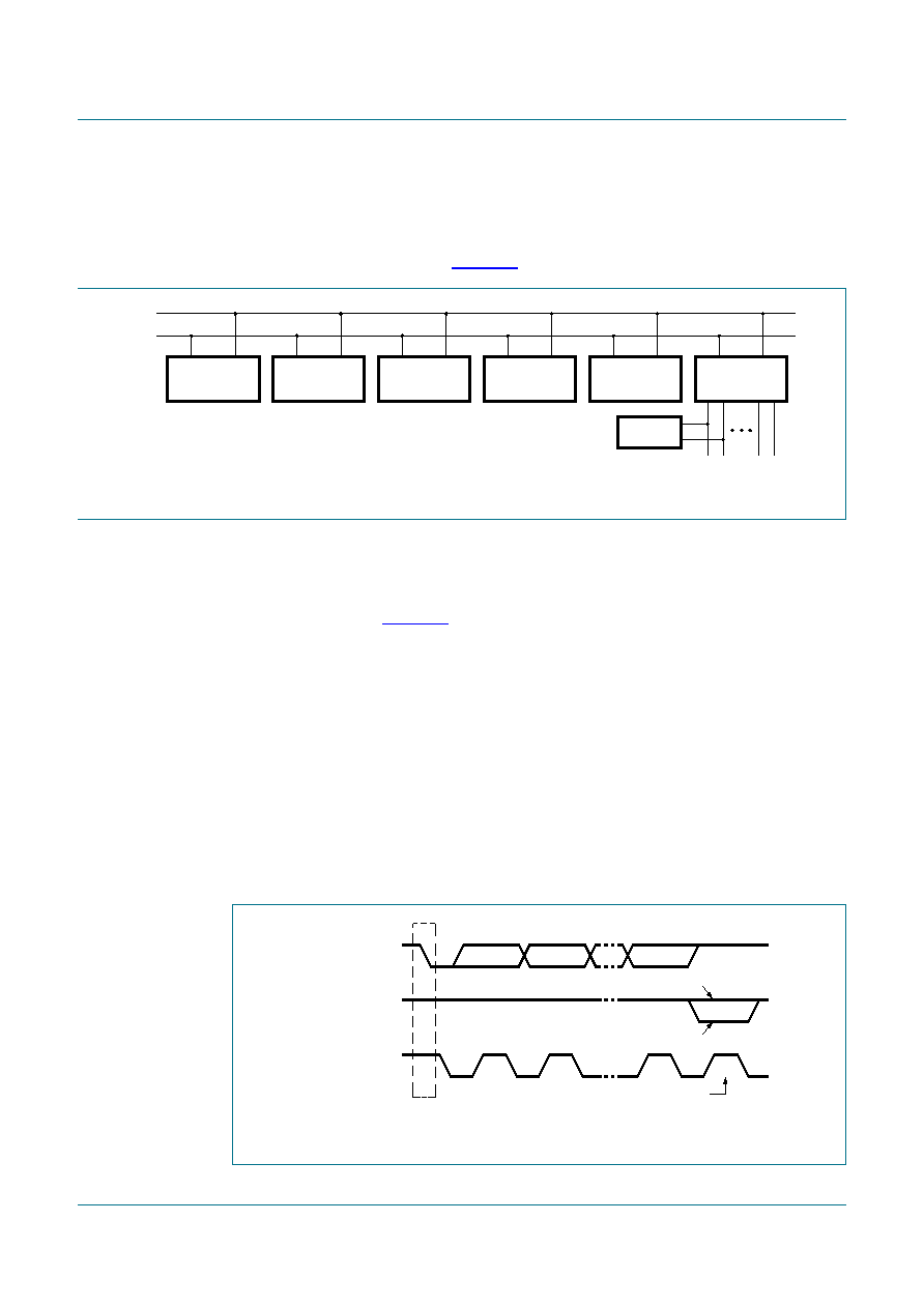
9.2 System configuration
A device generating a message is a ‘transmitter'; a device receiving is the ‘receiver'. The
device that controls the message is the ‘master' and the devices which are controlled by
the master are the ‘slaves' (see Figure 17).
9.3 Acknowledge
The number of data bytes transferred between the START and the STOP conditions from
transmitter to receiver is not limited. Each byte of eight bits is followed by one
acknowledge bit (see Figure 18). The acknowledge bit is an active LOW level (generated
by the receiving device) that indicates to the transmitter that the data transfer was
successful.
A slave receiver which is addressed must generate an acknowledge after the reception of
each byte. Also a master must generate an acknowledge after the reception of each byte
that has been clocked out of the slave transmitter. The device that wants to issue an
acknowledge bit has to pull down the SDA line during the acknowledge clock pulse, so
that the SDA line is stable LOW during the HIGH period of the acknowledge bit related
clock pulse; set-up and hold times must be taken into account.
A master receiver must signal an end of data to the transmitter by not generating an
acknowledge on the last byte that has been clocked out of the slave. In this event, the
transmitter must leave the data line HIGH to enable the master to generate a STOP
condition.
Fig 17. System configuration
002aaa966
MASTER
TRANSMITTER/
RECEIVER
SLAVE
RECEIVER
SLAVE
TRANSMITTER/
RECEIVER
MASTER
TRANSMITTER
MASTER
TRANSMITTER/
RECEIVER
SDA
SCL
I2C-BUS
MULTIPLEXER
SLAVE
Fig 18. Acknowledgement on the I2C-bus
002aaa987
S
START
condition
9
8
2
1
clock pulse for
acknowledgement
not acknowledge
acknowledge
data output
by transmitter
data output
by receiver
SCL from master
相关PDF资料 |
PDF描述 |
|---|---|
| PCA9574BS,118 | IC I/O EXPANDER I2C 8B 16HVQFN |
| ATTINY24A-MUR | MCU AVR 2KB FLASH 20MHZ 20QFN |
| PCA8574PW,118 | IC I/O EXPANDER I2C 8B 16TSSOP |
| ATTINY24A-CCUR | MCU AVR 2KB FLASH 20MHZ 15UFBGA |
| ATTINY24A-SSNR | MCU AVR 2KB FLASH 20MHZ 14SOIC |
相关代理商/技术参数 |
参数描述 |
|---|---|
| PCA9670PW-T | 功能描述:接口-I/O扩展器 8-BIT I2C FM+ QB GPIO INT PU RoHS:否 制造商:NXP Semiconductors 逻辑系列: 输入/输出端数量: 最大工作频率:100 kHz 工作电源电压:1.65 V to 5.5 V 工作温度范围:- 40 C to + 85 C 安装风格:SMD/SMT 封装 / 箱体:HVQFN-16 封装:Reel |
| PCA9671BQ,118 | 功能描述:接口-I/O扩展器 REMOTE 16BIT GPIO RoHS:否 制造商:NXP Semiconductors 逻辑系列: 输入/输出端数量: 最大工作频率:100 kHz 工作电源电压:1.65 V to 5.5 V 工作温度范围:- 40 C to + 85 C 安装风格:SMD/SMT 封装 / 箱体:HVQFN-16 封装:Reel |
| PCA9671BQ-T | 功能描述:接口-I/O扩展器 REMOTE 16BIT GPIO FM+I2C-RESET RoHS:否 制造商:NXP Semiconductors 逻辑系列: 输入/输出端数量: 最大工作频率:100 kHz 工作电源电压:1.65 V to 5.5 V 工作温度范围:- 40 C to + 85 C 安装风格:SMD/SMT 封装 / 箱体:HVQFN-16 封装:Reel |
| PCA9671BS,118 | 功能描述:接口-I/O扩展器 REMOTE 16BIT GPIO RoHS:否 制造商:NXP Semiconductors 逻辑系列: 输入/输出端数量: 最大工作频率:100 kHz 工作电源电压:1.65 V to 5.5 V 工作温度范围:- 40 C to + 85 C 安装风格:SMD/SMT 封装 / 箱体:HVQFN-16 封装:Reel |
| PCA9671BS-T | 功能描述:接口-I/O扩展器 REMOTE 16BIT GPIO FM+I2C-RESET RoHS:否 制造商:NXP Semiconductors 逻辑系列: 输入/输出端数量: 最大工作频率:100 kHz 工作电源电压:1.65 V to 5.5 V 工作温度范围:- 40 C to + 85 C 安装风格:SMD/SMT 封装 / 箱体:HVQFN-16 封装:Reel |
发布紧急采购,3分钟左右您将得到回复。