- 您现在的位置:买卖IC网 > PDF目录4212 > PCF8594C-2P/02,112 (NXP Semiconductors)IC EEPROM 4KBIT 100KHZ 8DIP PDF资料下载
参数资料
| 型号: | PCF8594C-2P/02,112 |
| 厂商: | NXP Semiconductors |
| 文件页数: | 7/21页 |
| 文件大小: | 0K |
| 描述: | IC EEPROM 4KBIT 100KHZ 8DIP |
| 标准包装: | 50 |
| 格式 - 存储器: | EEPROMs - 串行 |
| 存储器类型: | EEPROM |
| 存储容量: | 4K (512 x 8) |
| 速度: | 100kHz |
| 接口: | I²C,2 线串口 |
| 电源电压: | 2.5 V ~ 6.0 V |
| 工作温度: | -40°C ~ 85°C |
| 封装/外壳: | 8-DIP(0.300",7.62mm) |
| 供应商设备封装: | 8-DIP |
| 包装: | 管件 |
| 其它名称: | 568-3639-5 935195510112 PCF8594C2N |
�� �
�
�Philips� Semiconductors�
�PCF8594C-2�
�512� � 8-bit� CMOS� EEPROM� with� I� 2� C-bus� interface�
�The� master� receiver� must� generate� an� acknowledge� after� the� reception� of� each� byte�
�that� has� been� clocked� out� of� the� slave� transmitter.�
�The� device� that� acknowledges� has� to� pull� down� the� SDA� line� during� the� acknowledge�
�clock� pulse� in� such� a� way� that� the� SDA� line� is� stable� LOW� during� the� HIGH� period� of�
�the� acknowledge� related� clock� pulse.�
�Set-up� and� hold� times� must� be� taken� into� account.� A� master� receiver� must� signal� an�
�end� of� data� to� the� slave� transmitter� by� not� generating� an� acknowledge� on� the� last� byte�
�that� has� been� clocked� out� of� the� slave.� In� this� event,� the� transmitter� must� leave� the�
�data� line� HIGH� to� enable� the� master� generation� of� the� STOP� condition.�
�8.1.3�
�Device� addressing�
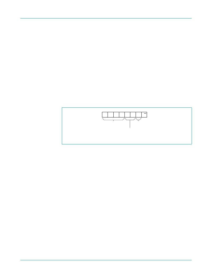
�Following� a� START� condition,� the� bus� master� must� output� the� address� of� the� slave� it�
�is� accessing.� The� address� of� the� PCF8594C-2� is� shown� in� Figure� 4� .� To� conserve�
�power,� no� internal� pull-up� resistors� are� incorporated� on� the� hardware� selectable� pins�
�and� they� must� be� connected� to� either� V� DD� or� V� SS� .�
�1�
�0�
�1�
�0�
�A2�
�A1�
�A0� R/W�
�FIXED�
�SOFTWARE�
�SELECTABLE�
�HARDWARE�
�SELECTABLE�
�002aaa261�
�Fig� 4.� Slave� address.�
�The� last� bit� of� the� slave� address� de?nes� the� operation� to� be� performed.� When� set� to�
�logic� 1,� a� read� operation� is� selected,� while� a� logic� 0� selects� a� write� operation.�
�9397� 750� 14221�
�8.1.4�
�Write� operations�
�A� write-protection� input� at� Pin� 1� (WP)� allows� disabling� of� write� commands� from� the�
�master� by� a� hardware� signal.� Write� accesses� are� allowed� to� either� the� upper� or� lower�
�256� bytes� of� the� EEPROM� if� the� pin� WP� is� LOW,� or� the� lower� 256� bytes� of� the�
�EEPROM� if� the� pin� WP� is� HIGH.� When� the� pin� WP� is� HIGH� the� upper� 256� bytes� of�
�the� EEPROM� are� write-protected� and� no� acknowledge� will� be� given� by� the�
�PCF8594C-2� when� data� is� sent.� However,� an� acknowledge� will� be� given� after� the�
�slave� address� and� the� word� address.�
�Byte/word� write:� For� a� write� operation,� the� PCF8594C-2� requires� a� second� address�
�?eld.� This� address� ?eld� is� a� word� address� providing� access� to� the� 256� words� of�
�memory.� Upon� receipt� of� the� word� address,� the� PCF8594C-2� responds� with� an�
�acknowledge� and� awaits� the� next� eight� bits� of� data,� again� responding� with� an�
�acknowledge.� Word� address� is� automatically� incremented.� The� master� can� now�
�terminate� the� transfer� by� generating� a� STOP� condition� or� transmit� up� to� six� more�
�bytes� of� data� and� then� terminate� by� generating� a� STOP� condition.�
�After� this� STOP� condition,� the� E/W� cycle� starts� and� the� bus� is� free� for� another�
�transmission.� Its� duration� is� 10� ms� per� byte.�
�During� the� E/W� cycle� the� slave� receiver� does� not� send� an� acknowledge� bit� if�
�addressed� via� the� I� 2� C-bus.�
�?� Koninklijke� Philips� Electronics� N.V.� 2004.� All� rights� reserved.�
�Product� data�
�Rev.� 05� —� 25� October� 2004�
�7� of� 21�
�相关PDF资料 |
PDF描述 |
|---|---|
| XC5VFX70T-1FF665I | IC FPGA VIRTEX-5FXT 665FFBGA |
| XC2V2000-6FFG896C | IC FPGA VIRTEX-II 2M 896-FBGA |
| XC2V2000-5FFG896I | IC FPGA VIRTEX-II 2M 896-FBGA |
| XC5VFX70T-1FFG665I | IC FPGA VIRTEX-5FX 70K 665-FCBGA |
| XC5VSX50T-1FFG1136I | IC FPGA VIRTEX-5 50K 1136FBGA |
相关代理商/技术参数 |
参数描述 |
|---|---|
| PCF8594C-2T | 制造商:NXP Semiconductors 功能描述:Bulk |
| PCF8594C-2T/02,112 | 功能描述:电可擦除可编程只读存储器 512X8 电可擦除可编程只读存储器 RoHS:否 制造商:Atmel 存储容量:2 Kbit 组织:256 B x 8 数据保留:100 yr 最大时钟频率:1000 KHz 最大工作电流:6 uA 工作电源电压:1.7 V to 5.5 V 最大工作温度:+ 85 C 安装风格:SMD/SMT 封装 / 箱体:SOIC-8 |
| PCF8594C-2T/02,118 | 功能描述:电可擦除可编程只读存储器 512X8 电可擦除可编程只读存储器 2.5V TO 6.0V RoHS:否 制造商:Atmel 存储容量:2 Kbit 组织:256 B x 8 数据保留:100 yr 最大时钟频率:1000 KHz 最大工作电流:6 uA 工作电源电压:1.7 V to 5.5 V 最大工作温度:+ 85 C 安装风格:SMD/SMT 封装 / 箱体:SOIC-8 |
| PCF8594C-2T/02112 | 制造商:Rochester Electronics LLC 功能描述: 制造商:NXP 功能描述: 制造商:NXP Semiconductors 功能描述: |
| PCF8594C-2T02 | 制造商:PHILIPS 制造商全称:NXP Semiconductors 功能描述:512 X 8-bit CMOS EEPROM with I2C-bus interface |
发布紧急采购,3分钟左右您将得到回复。