- 您现在的位置:买卖IC网 > PDF目录190038 > PE42612-91 (PEREGRINE SEMICONDUCTOR CORP) SP4T UltraCMOS 2.6 V Switch 100 - 3000 MHz PDF资料下载
参数资料
| 型号: | PE42612-91 |
| 厂商: | PEREGRINE SEMICONDUCTOR CORP |
| 元件分类: | 开关 |
| 英文描述: | SP4T UltraCMOS 2.6 V Switch 100 - 3000 MHz |
| 中文描述: | 100 MHz - 3000 MHz RF/MICROWAVE SGL POLE FOUR THROW SWITCH, 1.2 dB INSERTION LOSS |
| 封装: | FLIP CHIP-12 |
| 文件页数: | 2/4页 |
| 文件大小: | 158K |
| 代理商: | PE42612-91 |
Product Brief
PE42612
Page 2 of 4
2006 Peregrine Semiconductor Corp. All rights reserved.
Document No. 70-0217-01
│ UltraCMOS RFIC Solutions
Contact sales@psemi.com for full version of datasheet
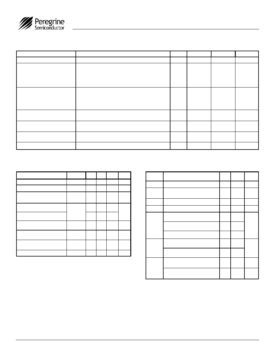
Table 2. Operating Ranges
Table 3. Absolute Maximum Ratings
Table 1. PE42612 Electrical Specifications: Temp = 25°C, VDD = 2.6 V
Parameter
Condition
Min
Typ
Max
Unit
Operational Frequency
100
3000
MHz
Insertion Loss
ANT - TX - 850 / 900 MHz
ANT - TX - 1800 / 1900 MHz
ANT - RX - 850 / 900 MHz
ANT - RX - 1800 / 1900 MHz
0.55
0.7
0.85
1.05
0.65
0.8
1.0
1.2
dB
Isolation
TX - RX - 850 / 900 MHz (TX ON)
TX - RX - 1800 / 1900 MHz (TX ON)
TX1 - TX2 - 850 / 900 MHz (TX1 ON)
TX1 - TX2 - 1800 / 1900 MHz (TX1 ON)
37
29
33
26
39
31
35
28
dB
Return Loss
850 / 900 MHz
1800 / 1900 MHz
18
14
20
16
dB
2nd Harmonic1,2
35 dBm TX Input Power - 850 / 900 MHz
33 dBm TX Input Power - 1800 / 1900 MHz
-82
-89
-78
-82
dBc
3rd Harmonic1,2
35 dBm TX Input Power - 850 / 900 MHz
33 dBm TX Input Power - 1800 / 1900 MHz
-74
-68
-69
-65
dBc
Switching time
(10-90%) (90-10%) RF
2
3
s
Notes:
1. Measured in Pulsed Wave Mode.
2. Assumes RF input duty cycle of 50% and 4620
s, measured per 3GPP TS 45.005
Parameter
Symbol
Min Typ Max Units
Temperature range
TOP
-40
+85
°C
VDD Supply Voltage
VDD
2.4
2.6
2.95
V
IDD Power Supply Current
(VDD = 2.6 V)
IDD
11
25
A
TX input power (VSWR
≤ 3:1)
824-915 MHz
+35
dBm
+33
RX input power
(VSWR
≤1:1)
PIN
+20
dBm
Control Voltage High
VIH
1.40
V
Control Voltage Low
VIL
0.40
V
PIN
TX input power (VSWR
≤ 3:1)
1710-1910 MHz
Control Line Current
1
A
Symbol
Parameter/Conditions
Min
Max
Units
VDD
Power supply voltage
-0.3
4.0
V
VI
Voltage on any DC input
-0.3
VDD+
0.3
V
TST
Storage temperature range
-65
+150
°C
TOP
Operating temperature range
-40
+85
°C
PIN
TX input power (50
)3,4
824-915 MHz
+38
dBm
TX input power (50
)3,4
1710-1910 MHz
+36
RX input power (50
)
+23
PIN (∞:1)
TX input power (VSWR = (
∞:1)3,4
824-915 MHz
+35
dBm
TX input power (VSWR = (
∞:1)3,4
1710-1910 MHz
+33
VESD
ESD Voltage (HBM, MIL_STD
883 Method 3015.7)
1500
V
ESD Voltage (MM, JEDEC,
JESD22-A114-B)
100
V
Note:
3. Assumes RF input duty cycle of 50% and 4620
s.
4. VDD within operating range specified in Table 4.
Absolute Maximum Ratings are those values listed in
the above table. Exceeding these values may cause
permanent device damage. Functional operation
should be restricted to the limits in the DC Electrical
Specifications table. Exposure to absolute maximum
ratings for extended periods may affect device
reliability.
相关PDF资料 |
PDF描述 |
|---|---|
| PE4261 | SP4T UltraCMOS⑩ 2.6 V Switch 100 - 3000 MHz |
| PE42632DBI | SP6T UltraCMOS 2.70 V Switch 100 - 3000 MHz,50ohm |
| PE42632DTI | SP6T UltraCMOS 2.70 V Switch 100 - 3000 MHz,50ohm |
| PE4263 | SP6T UltraCMOS⑩ 2.6 V Switch 100 - 3000 MHz |
| PE42674DBI | SP7T UltraCMOS WEDGE Switch 100 -3000 MHz, +67 dBm IIP3 |
相关代理商/技术参数 |
参数描述 |
|---|---|
| PE4261-93 | 制造商:PEREGRINE 制造商全称:PEREGRINE 功能描述:SP4T UltraCMOS⑩ 2.6 V Switch 100 - 3000 MHz |
| PE4261-96 | 制造商:PEREGRINE 制造商全称:PEREGRINE 功能描述:SP4T UltraCMOS⑩ 2.6 V Switch 100 - 3000 MHz |
| PE4262 | 制造商:MISC. CONNECTORS 功能描述: |
| PE4263 | 制造商:PEREGRINE 制造商全称:PEREGRINE 功能描述:SP6T UltraCMOS? 2.6 V Switch 100 - 3000 MHz |
| PE42632 | 制造商:PEREGRINE 制造商全称:PEREGRINE 功能描述:SP6T UltraCMOS 2.70 V Switch 100 - 3000 MHz,50ohm |
发布紧急采购,3分钟左右您将得到回复。