- 您现在的位置:买卖IC网 > PDF目录369994 > PF48F2000P0ZTQ0 (INTEL CORP) Intel StrataFlash Embedded Memory PDF资料下载
参数资料
| 型号: | PF48F2000P0ZTQ0 |
| 厂商: | INTEL CORP |
| 元件分类: | PROM |
| 英文描述: | Intel StrataFlash Embedded Memory |
| 中文描述: | 4M X 16 FLASH 1.8V PROM, 85 ns, PBGA88 |
| 封装: | 8 X 10 MM, 1.20 MM HEIGHT, LEAD FREE, SCSP-88 |
| 文件页数: | 61/102页 |
| 文件大小: | 1609K |
| 代理商: | PF48F2000P0ZTQ0 |
第1页第2页第3页第4页第5页第6页第7页第8页第9页第10页第11页第12页第13页第14页第15页第16页第17页第18页第19页第20页第21页第22页第23页第24页第25页第26页第27页第28页第29页第30页第31页第32页第33页第34页第35页第36页第37页第38页第39页第40页第41页第42页第43页第44页第45页第46页第47页第48页第49页第50页第51页第52页第53页第54页第55页第56页第57页第58页第59页第60页当前第61页第62页第63页第64页第65页第66页第67页第68页第69页第70页第71页第72页第73页第74页第75页第76页第77页第78页第79页第80页第81页第82页第83页第84页第85页第86页第87页第88页第89页第90页第91页第92页第93页第94页第95页第96页第97页第98页第99页第100页第101页第102页
1-Gbit P30 Family
Datasheet
Intel StrataFlash
Embedded Memory (P30)
Order Number: 306666, Revision: 001
April 2005
61
11.0
Programming Operations
The device supports three programming methods: Word Programming (40h/10h), Buffered
Programming (E8h, D0h), and Buffered Enhanced Factory Programming (80h, D0h). See
Section
9.0, “Device Operations” on page 48
for details on the various programming commands issued to
the device. The following sections describe device programming in detail.
Successful programming requires the addressed block to be unlocked. If the block is locked down,
WP# must be deasserted and the block must be unlocked before attempting to program the block.
Attempting to program a locked block causes a program error (SR[4] and SR[1] set) and
termination of the operation. See
Section 13.0, “Security Modes” on page 69
for details on locking
and unlocking blocks.
The Intel StrataFlash Embedded Memory (P30) is segmented into multiple Programming
Regions. Programming Regions are made up of 8 or 16 blocks depending on the density. The 64-
and 128-Mbit devices have 8 blocks per Programming Region, while the 256-Mbit has 16 blocks in
each Programming Region (see
Table 26
). See
Section 4.4, “Memory Maps” on page 24
for
address ranges of each Programming Region per density.
Execute in Place (XIP) is defined as the ability to execute code directly from the flash memory.
XIP applications must partition the memory such that code and data are in separate programming
regions (see
Table 26, “Programming Regions per Device” on page 61
). Each Programming
Region should contain only code or data, and not both. The following terms define the difference
between code and data. System designs must use these definitions when partitioning their code and
data for the P30 device.
11.1
Word Programming
Word programming operations are initiated by writing the Word Program Setup command to the
device (see
Section 9.0, “Device Operations” on page 48
). This is followed by a second write to the
device with the address and data to be programmed. The device outputs Status Register data when
read. See
Figure 40, “Word Program Flowchart” on page 85
. V
PP
must be above V
PPLK
, and within
the specified V
PPL
min/max values (nominally 1.8 V).
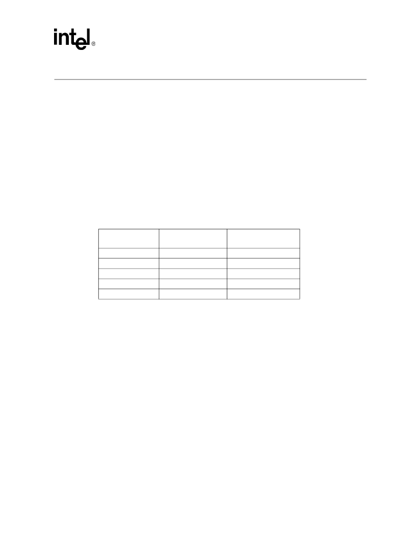
Table 26.
Programming Regions per Device
Device Density
Number of blocks per
Programming Region
Number of Programming
Regions per Device
64-Mbit
8 blocks
8
128-Mbit
8 blocks
16
256-Mbit
16 blocks
16
512-Mbit
16 blocks
32
1-Gbit
16 blocks
64
Code :
Execution code ran out of the flash device on a continuous basis in the system.
Data :
Information periodically programmed into the flash device and read back (e.g.
execution code shadowed and executed in RAM, pictures, log files, etc.).
相关PDF资料 |
PDF描述 |
|---|---|
| PF48F3000P0ZTQ0 | Circular Connector; Body Material:Aluminum; Series:PT00; No. of Contacts:6; Connector Shell Size:10; Connecting Termination:Solder; Circular Shell Style:Wall Mount Receptacle; Circular Contact Gender:Pin; Insert Arrangement:10-6 |
| PF48F4000P0ZTQ0 | Circular Connector; MIL SPEC:MIL-C-26482, Series I, Solder; Body Material:Aluminum; Series:PT00; Number of Contacts:6; Connector Shell Size:10; Connecting Termination:Solder; Circular Shell Style:Wall Mount Receptacle |
| PF48F0P0ZTQ0 | Circular Connector; Body Material:Aluminum; Series:PT00; No. of Contacts:6; Connector Shell Size:10; Connecting Termination:Solder; Circular Shell Style:Wall Mount Receptacle; Circular Contact Gender:Socket; Insert Arrangement:10-98 |
| PF48F2P0ZTQ0 | Circular Connector; MIL SPEC:MIL-C-26482, Series I, Solder; Body Material:Aluminum; Series:PT00; No. of Contacts:10; Connector Shell Size:12; Connecting Termination:Solder; Circular Shell Style:Wall Mount Receptacle |
| PF48F3P0ZTQ0 | Circular Connector; Body Material:Aluminum; Series:PT00; No. of Contacts:10; Connector Shell Size:12; Connecting Termination:Solder; Circular Shell Style:Wall Mount Receptacle; Circular Contact Gender:Pin; Insert Arrangement:12-10 |
相关代理商/技术参数 |
参数描述 |
|---|---|
| PF48F2000P0ZTQ0A | 功能描述:IC FLASH 64MBIT 85NS 88TPBGA RoHS:是 类别:集成电路 (IC) >> 存储器 系列:StrataFlash™ 标准包装:3,000 系列:- 格式 - 存储器:EEPROMs - 串行 存储器类型:EEPROM 存储容量:32K (4K x 8) 速度:100kHz,400kHz 接口:I²C,2 线串口 电源电压:2.5 V ~ 5.5 V 工作温度:-40°C ~ 125°C 封装/外壳:8-SOIC(0.154",3.90mm 宽) 供应商设备封装:8-SOIC 包装:带卷 (TR) 其它名称:CAV24C32WE-GT3OSTR |
| PF48F2000W0YTQE | 制造商:Micron Technology Inc 功能描述:64X/0X QUAD 1.8 HF CUOSP - Tape and Reel |
| PF48F2000W0YTQEA | 制造商:Micron Technology Inc 功能描述:64X/0X QUAD 1.8 HF CUOSP - Trays |
| PF48F2P0VB00 | 制造商:INTEL 制造商全称:Intel Corporation 功能描述:Intel StrataFlash Embedded Memory |
| PF48F2P0VBQ0 | 制造商:INTEL 制造商全称:Intel Corporation 功能描述:Intel StrataFlash Embedded Memory |
发布紧急采购,3分钟左右您将得到回复。