- 您现在的位置:买卖IC网 > PDF目录69043 > PFS716EG (POWER INTEGRATIONS INC) POWER FACTOR CONTROLLER, 95 kHz SWITCHING FREQ-MAX, PZIP6 PDF资料下载
参数资料
| 型号: | PFS716EG |
| 厂商: | POWER INTEGRATIONS INC |
| 元件分类: | 稳压器 |
| 英文描述: | POWER FACTOR CONTROLLER, 95 kHz SWITCHING FREQ-MAX, PZIP6 |
| 封装: | HALOGEN FREE AND ROHS COMPLIANT, PLASTIC, SIP-7/6 |
| 文件页数: | 25/30页 |
| 文件大小: | 2647K |
| 代理商: | PFS716EG |
第1页第2页第3页第4页第5页第6页第7页第8页第9页第10页第11页第12页第13页第14页第15页第16页第17页第18页第19页第20页第21页第22页第23页第24页当前第25页第26页第27页第28页第29页第30页
Rev. A 11/09/10
4
PFS704-729EG
www.powerint.com
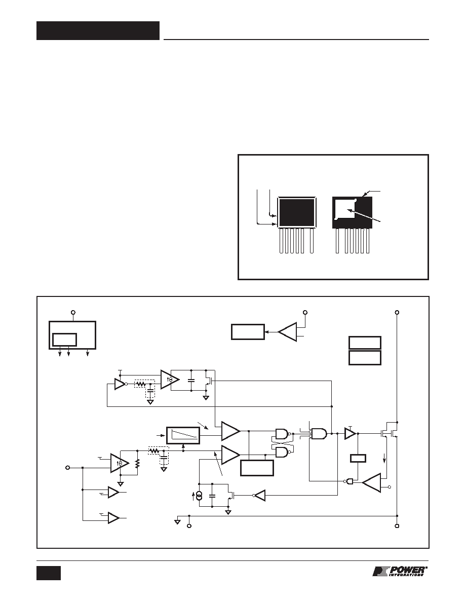
Figure 3.
Functional Block Diagram.
Pin Functional Description
VOLTAGE MONITOR (V) Pin:
The V pin is tied to the rectified AC rail through an external
resistor. Internal circuitry detects the peak of the input line
voltage which resembles a full-wave rectified waveform. The
rectified high-voltage bus is connected directly to the V pin
voltage through a large resistor (4 M
W for PFS70x and PFS71x;
9 M
W for PFS72x) to minimize power dissipation and standby
power consumption. A small ceramic capacitor (0.1
mF for
PFS70x and PFS71x; 0.047
mF for PFS72x) is required from the
VOLTAGE MONITOR pin to SIGNAL GROUND pin to bypass
any switching noise present on the rectified bus. This pin also
features both brown-in and brown-out protection.
FEEDBACK (FB) Pin:
The FEEDBACK pin is high input-impedance reference terminal
that connects to a feedback resistor network. This pin will also
feature fast overvoltage and undervoltage detection circuitry
that will disengage the internal power MOSFET in the event of a
system fault. A 10 nF capacitor is required between the
FEEDBACK to SIGNAL GROUND pins; this capacitor must be
placed very close to the device on the PCB to bypass any
switching noise. This pin is also used for loop compensation.
BIAS POWER (VCC) Pin:
This is a 10-12 VDC bias supply used to power the IC. The bias
voltage must be externally clamped to prevent the VCC pin
from exceeding 13.4 VDC.
SIGNAL GROUND (G) Pin:
Discrete components used in the feedback circuit, including
loop compensation, decoupling capacitors for the supply (VCC)
and line-sense (V) must be referenced to the G pin.
The
SIGNAL GROUND pin must not be tied to the SOURCE pin.
SOURCE (S) Pin:
This pin is the source connection of the power switch.
DRAIN (D) Pin:
This is the tab and drain connection of the internal power switch.
Figure 2.
Pin Configuration.
PI-5333-113010
+
-
+
-
+
-
+
-
“Off-time derived with
constant Volt-Sec
Input Voltage
Emulation
VOFF is a function of the error-voltage (VE) and is used to reduce the average
operating frequency as a function of output power for increased efficiency
(PFS704-716).
(VOFF = 0.8 V for PFS723-729).
The internal derived error-voltage (VE)
regulates the output voltage
MON is the switch current
sense scale factor which
is function of peak line
voltage derived from IVIN
Fast OV
Comparator
FB
OV/UV
OTP
VCC
VOLTAGE MONITOR (V)
SIGNAL GROUND (G)
SOURCE (S)
BIAS POWER (VCC)
DRAIN (D)
FEEDBACK (FB)
FB
UV/
FB
OFF
VCC+
MON
Internal
Reference
V
REF
Transconductance
Error-Amplifier
Driver
I
OCP
Sense
FET
Power
MOSFET
UV Comparator
TIMER
SUPERVISOR
INPUT
LINE INTERFACE
Peak
Detector
INTERNAL
SUPPLY
OTP
SOFT
START
+
-
+
-
+
-
+
-
6 V
CINT
MON IS
CINT
VO-VIN
IVPK
Input UV
(IUV-/IUV+)
IS
LEB
OCP
1 kHz
Filter
7 kHz
Filter
Comparator
VOFF
V
OFF
VE
V
E
Frequency
Slide
Comparator
Latch
Input UV
FB
OV
PI-5334-083110
Exposed Pad
(Backside)
Internally
Connected to
DRAIN Pin
(see eSIP-7G
Package
Drawing)
Exposed Metal
(On Edge)
Internally
Connected to
DRAIN Pin
Exposed Metal (On Edge)
Internally Connected
to GROUND Pin
E Package (eSIP-7G)
1 2 3 4 5
7
V FB VCC G S
D
7
5 4 3 2 1
D
S G VCC FB V
相关PDF资料 |
PDF描述 |
|---|---|
| PFS708EG | POWER FACTOR CONTROLLER, 95 kHz SWITCHING FREQ-MAX, PZIP6 |
| PFS729EG | POWER FACTOR CONTROLLER, 95 kHz SWITCHING FREQ-MAX, PZIP6 |
| PFS724EG | POWER FACTOR CONTROLLER, 95 kHz SWITCHING FREQ-MAX, PZIP6 |
| PFS706EG | POWER FACTOR CONTROLLER, 95 kHz SWITCHING FREQ-MAX, PZIP6 |
| PFS723EG | POWER FACTOR CONTROLLER, 95 kHz SWITCHING FREQ-MAX, PZIP6 |
相关代理商/技术参数 |
参数描述 |
|---|---|
| PFS723EG | 功能描述:功率因数校正 IC PFC w/ Pwr Mosfet 280 W MAX 180 VAC RoHS:否 制造商:Fairchild Semiconductor 开关频率:300 KHz 最大功率耗散: 最大工作温度:+ 125 C 安装风格:SMD/SMT 封装 / 箱体:SOIC-8 封装:Reel |
| PFS724EG | 功能描述:功率因数校正 IC PFC w/ Pwr Mosfet 350 W MAX 180 VAC RoHS:否 制造商:Fairchild Semiconductor 开关频率:300 KHz 最大功率耗散: 最大工作温度:+ 125 C 安装风格:SMD/SMT 封装 / 箱体:SOIC-8 封装:Reel |
| PFS725EG | 功能描述:功率因数校正 IC PFC w/ Pwr Mosfet 480 W MAX 180 VAC RoHS:否 制造商:Fairchild Semiconductor 开关频率:300 KHz 最大功率耗散: 最大工作温度:+ 125 C 安装风格:SMD/SMT 封装 / 箱体:SOIC-8 封装:Reel |
| PFS726EG | 功能描述:功率因数校正 IC PFC w/ Pwr Mosfet 600 W MAX 180 VAC RoHS:否 制造商:Fairchild Semiconductor 开关频率:300 KHz 最大功率耗散: 最大工作温度:+ 125 C 安装风格:SMD/SMT 封装 / 箱体:SOIC-8 封装:Reel |
| PFS727EG | 功能描述:功率因数校正 IC PFC w/ Pwr Mosfet 750 W MAX 180 VAC RoHS:否 制造商:Fairchild Semiconductor 开关频率:300 KHz 最大功率耗散: 最大工作温度:+ 125 C 安装风格:SMD/SMT 封装 / 箱体:SOIC-8 封装:Reel |
发布紧急采购,3分钟左右您将得到回复。