- 您现在的位置:买卖IC网 > PDF目录69043 > PFS716EG (POWER INTEGRATIONS INC) POWER FACTOR CONTROLLER, 95 kHz SWITCHING FREQ-MAX, PZIP6 PDF资料下载
参数资料
| 型号: | PFS716EG |
| 厂商: | POWER INTEGRATIONS INC |
| 元件分类: | 稳压器 |
| 英文描述: | POWER FACTOR CONTROLLER, 95 kHz SWITCHING FREQ-MAX, PZIP6 |
| 封装: | HALOGEN FREE AND ROHS COMPLIANT, PLASTIC, SIP-7/6 |
| 文件页数: | 6/30页 |
| 文件大小: | 2647K |
| 代理商: | PFS716EG |
第1页第2页第3页第4页第5页当前第6页第7页第8页第9页第10页第11页第12页第13页第14页第15页第16页第17页第18页第19页第20页第21页第22页第23页第24页第25页第26页第27页第28页第29页第30页
Rev. A 11/09/10
14
PFS704-729EG
www.powerint.com
PI-6228-111110
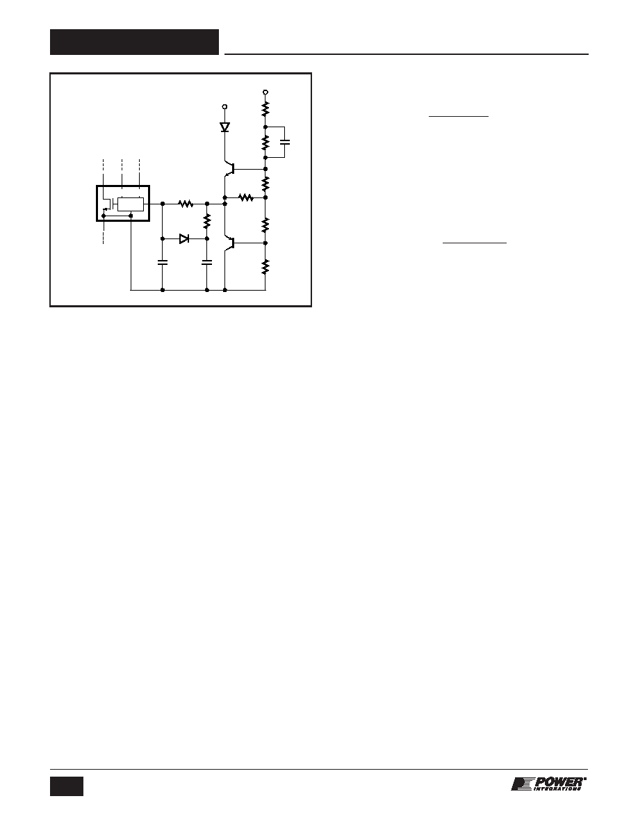
D1
D2
R8
R1
R2
R3
R6
Q1
Q2
R4
R5
D
S
FB
VCC
V
G
CONTROL
HiperPFS
C3
C2
C1
B+
VCC
R7
R7 and capacitor C2 is the loop compensation network which
introduces a low frequency zero required to tailor the loop
response to ensure low cross-over frequency and sufficient
phase margin. Resistor R6 isolates the fast portion (resistor
voltage divider network comprising of resistors R1 to R5) and
the slow feedback loop compensator circuit (resistor R7 and
capacitor C2). Transistors Q1 and Q2, biased with resistors R3
and R4 respectively, detect output voltage transient conditions
and provide the FEEDBACK pin with “fast” information to
increase the loop response of the system. Diode D1 is included
to cover a single point fault condition wherein capacitor C2 is
shorted. In the event C2 is short-circuited, the FEEDBACK pin
is forced below the FB
OFF threshold through diode D1 and
subsequently turns the HiperPFS off. Only a standard recovery
diode should be used for D1. Use of ultrafast or fast recovery
diode is not recommended including small signal diodes (e.g.
1N4148) which are typically also fast recovery.
The recommended values for the components used are as
follows:
R5 = 57.6 k
W
R3, R4 = 2.2 k
W
R2 = 732 k
W
C1 = 0.1
mF, 100 V X7R/NPO
R6 = 160 k
W
R7 = 3 k
W
R8 = 2 k
W
C2 = 4.7
mF
C3 = 10 nF (For layouts that result in excessive noise on the
feedback signal, a 20 nF capacitor may be used).
D1 = BAV116 W or 1N4007 (A general purpose standard
recovery diode should only be used).
Q1, Q2 = Small signal transistors equivalent to 2N4401 and
2N4403.
Figure 14. Recommended Feedback Circuit.
When the above component values are used, the value of
resistor R1 can be calculated using the equation below:
R
V
100
10
79
O
1
6
#
=
-
Since the total voltage across resistor R1 is approximately
301 V, resistor R1 may have to be divided into two or more
resistors to distribute the voltage stress below the voltage
ratings of the resistor used.
The value of resistor R7 will have to be adjusted in some
designs and as a guideline the value from the following
calculation can be used:
R
V
C
P
k
4
Z
O
7
2
#
X
=
^ h
P
O
Maximum continuous output power in watts
V
O
Nominal PFC output voltage in volts
C
O
PFC output capacitance in farads
Improvement in low frequency phase margin can be achieved by
increasing the value of the capacitor C2 however increase in value
of capacitor C2 will result in some increase in overshoot at the
output of the PFC during transient loading and should be verified.
Diode D2 connected in series with the collector of the NPN
transistor Q1 is to prevent loading of the feedback circuit when
the V
CC is absent. Presence of this diode ensures that there is
no start-up delay when the V
CC is applied to the HiperPFS, the
feedback circuit, and transistor.
Heat Sinking and Thermal Design
The exposed pad on the HiperPFS eSIP package is internally
connected to the drain of the MOSFET. Due to the significant
amount of power dissipated in the part, the HiperPFS should be
mounted on a rectangular heat spreader made of thermally
conductive material such as Aluminum or Copper. Figure 15
shows an example of the recommended assembly for the
HiperPFS. In this assembly shown, a 0.76 mm thick aluminum
heat spreader is used. A thermally conductive sil pad should be
used to separate the heat spreader from the heat sink. A thin
film of thermally conductive silicone grease should be applied to
the rear surface of the HiperPFS to ensure low thermal
resistance contact between the package of the HiperPFS and
the heat spreader.
For universal input applications up to 150 W and 230 VAC only
applications up to 300 W, the heat spreader is not essential.
Use of heat spreader in these applications will help reduce
temperature of the part and heat spreaders can be used if
necessary. Figure 17 shows an example of the recommended
assembly for lower power designs that do not need a heat
spreader.
The HiperPFS is electrically connected to the heat spreader and
the heat sink is required to be connected to the source in order
to reduce EMI. The voltage between the heat spreader and
heat sink can easily exceed 400 V during transient conditions.
Attention should be placed on creepage and clearance based
on applicable safety specification.
相关PDF资料 |
PDF描述 |
|---|---|
| PFS708EG | POWER FACTOR CONTROLLER, 95 kHz SWITCHING FREQ-MAX, PZIP6 |
| PFS729EG | POWER FACTOR CONTROLLER, 95 kHz SWITCHING FREQ-MAX, PZIP6 |
| PFS724EG | POWER FACTOR CONTROLLER, 95 kHz SWITCHING FREQ-MAX, PZIP6 |
| PFS706EG | POWER FACTOR CONTROLLER, 95 kHz SWITCHING FREQ-MAX, PZIP6 |
| PFS723EG | POWER FACTOR CONTROLLER, 95 kHz SWITCHING FREQ-MAX, PZIP6 |
相关代理商/技术参数 |
参数描述 |
|---|---|
| PFS723EG | 功能描述:功率因数校正 IC PFC w/ Pwr Mosfet 280 W MAX 180 VAC RoHS:否 制造商:Fairchild Semiconductor 开关频率:300 KHz 最大功率耗散: 最大工作温度:+ 125 C 安装风格:SMD/SMT 封装 / 箱体:SOIC-8 封装:Reel |
| PFS724EG | 功能描述:功率因数校正 IC PFC w/ Pwr Mosfet 350 W MAX 180 VAC RoHS:否 制造商:Fairchild Semiconductor 开关频率:300 KHz 最大功率耗散: 最大工作温度:+ 125 C 安装风格:SMD/SMT 封装 / 箱体:SOIC-8 封装:Reel |
| PFS725EG | 功能描述:功率因数校正 IC PFC w/ Pwr Mosfet 480 W MAX 180 VAC RoHS:否 制造商:Fairchild Semiconductor 开关频率:300 KHz 最大功率耗散: 最大工作温度:+ 125 C 安装风格:SMD/SMT 封装 / 箱体:SOIC-8 封装:Reel |
| PFS726EG | 功能描述:功率因数校正 IC PFC w/ Pwr Mosfet 600 W MAX 180 VAC RoHS:否 制造商:Fairchild Semiconductor 开关频率:300 KHz 最大功率耗散: 最大工作温度:+ 125 C 安装风格:SMD/SMT 封装 / 箱体:SOIC-8 封装:Reel |
| PFS727EG | 功能描述:功率因数校正 IC PFC w/ Pwr Mosfet 750 W MAX 180 VAC RoHS:否 制造商:Fairchild Semiconductor 开关频率:300 KHz 最大功率耗散: 最大工作温度:+ 125 C 安装风格:SMD/SMT 封装 / 箱体:SOIC-8 封装:Reel |
发布紧急采购,3分钟左右您将得到回复。