参数资料
| 型号: | PI6C2408-1WIE |
| 厂商: | Pericom |
| 文件页数: | 9/10页 |
| 文件大小: | 0K |
| 描述: | IC 4+4 0-DELAY CLK BUFF 16-SOIC |
| 产品变化通告: | Product Discontinuation Notice 22/Jan/2010 |
| 标准包装: | 48 |
| 类型: | 零延迟缓冲器 |
| PLL: | 带旁路 |
| 输入: | TTL |
| 输出: | TTL |
| 电路数: | 1 |
| 比率 - 输入:输出: | 1:8 |
| 差分 - 输入:输出: | 无/无 |
| 频率 - 最大: | 140MHz |
| 除法器/乘法器: | 无/无 |
| 电源电压: | 3.135 V ~ 3.465 V |
| 工作温度: | -40°C ~ 85°C |
| 安装类型: | 表面贴装 |
| 封装/外壳: | 16-SOIC(0.154",3.90mm 宽) |
| 供应商设备封装: | 16-SOIC |
| 包装: | 管件 |
2006 Fairchild Semiconductor Corporation
www.fairchildsemi.com
FMS6690 Rev. 1.0.3
8
FM
S6690
—
Six
C
h
annel,
6
th
Order,
SD/PS/HD
Video
Filt
er
Driver
Applications Information
Functional Description
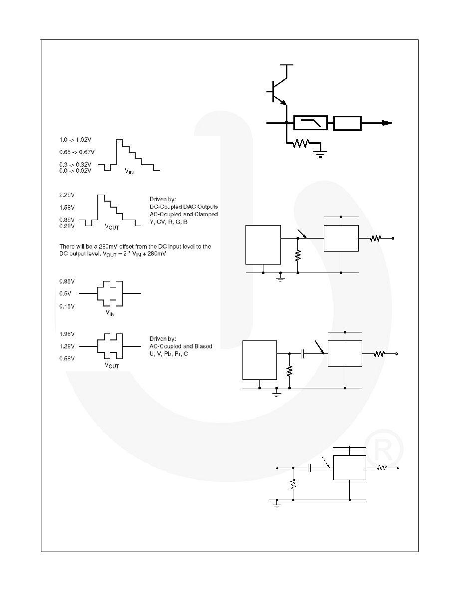
The FMS6690 Low-Cost Video Filter (LCVF) provides
6dB gain (9dB optional, contact factory for further
information) from input to output. In addition, the input is
slightly offset to optimize the output driver performance.
The offset is held to the minimum required value to
decrease the standing DC current into the load. Typical
voltage levels are shown in Figure 14.
Figure 14. Typical Voltage Levels
The FMS6690 provides an internal diode clamp to
support AC-coupled input signals. If the input signal
does not go below ground, the input clamp does not
operate. This allows DAC outputs to directly drive the
FMS6690 without an AC coupling capacitor. The worst-
case sync tip compression, due to the clamp, does not
exceed 7mV. The input level set by the clamp,
combined with the internal DC offset, keeps the output
within acceptable range. When the input is AC-coupled,
the diode clamp sets the sync tip (or lowest voltage) just
below ground.
For symmetric signals like C, U, V, Cb, Cr, Pb, and Pr;
the average DC bias is fairly constant and the inputs
can be AC-coupled with the addition of a pull-up resistor
to set the DC input voltage. DAC outputs can also drive
these same signals without the AC coupling capacitor.
A conceptual illustration of the input clamp circuit is
shown in Figure 15.
YOUT
800k
Driver
YIN
0.65V
Figure 15. Input Clamp Circuit
I/O Configurations
For DC-coupled DAC drive with DC-coupled outputs,
use the configuration in Figure 16.
DVD or
STB
SoC
DAC
Output
75
Ω
LCVF
Clamp
Inactive
0V- 1.4V
Figure 16. DC-Coupled Inputs and Outputs
Alternatively, if the DAC’s average DC output level
causes the signal to exceed the range of 0V to 1.4V, it
can be AC-coupled, as shown in Figure 17.
DVD or
STB
SoC
DAC
Output
75
Ω
LCVF
Clamp
Active
0.1
0V- 1.4V
Figure 17. AC-Coupled Inputs, DC-coupled Outputs
When the FMS6690 is driven by an unknown external
source or a SCART with its own clamping circuitry, the
inputs should be AC-coupled, shown in Figure 18.
75
Ω
LCVF
Clamp
Active
75
Ω
0.1
External Video
source must
be AC-coupled.
0V- 1.4V
Figure 18. SCART with DC-Coupled Outputs
相关PDF资料 |
PDF描述 |
|---|---|
| VI-24R-MW-F4 | CONVERTER MOD DC/DC 7.5V 100W |
| MS17343R36N5P | CONN RCPT 4POS WALL MT W/PINS |
| MS17346R28C10S | CONN RCPT 7POS BOX MT W/SCKT |
| PI6C2408-1WE | IC 4+4 0-DELAY CLK BUFF 16-SOIC |
| VI-24R-MW-F3 | CONVERTER MOD DC/DC 7.5V 100W |
相关代理商/技术参数 |
参数描述 |
|---|---|
| PI6C2408-1WIEX | 功能描述:锁相环 - PLL 4+4 Zero Delay Clock Buffer RoHS:否 制造商:Silicon Labs 类型:PLL Clock Multiplier 电路数量:1 最大输入频率:710 MHz 最小输入频率:0.002 MHz 输出频率范围:0.002 MHz to 808 MHz 电源电压-最大:3.63 V 电源电压-最小:1.71 V 最大工作温度:+ 85 C 最小工作温度:- 40 C 封装 / 箱体:QFN-36 封装:Tray |
| PI6C2408-2 | 制造商:未知厂家 制造商全称:未知厂家 功能描述:Clock IC | 4+4 Output Zero-Delay Clock Driver(Bank A = Ref. Bank B=Ref/2). 10 to 134 MHz |
| PI6C2408-2I | 制造商:未知厂家 制造商全称:未知厂家 功能描述:Clock IC | 4+4 Output Zero-Delay Clock Driver (Bank A = Ref. Bank B=Ref/2). 10 to 134 MHz. Industrial Temp. Operation |
| PI6C2408-2W | 制造商:PERICOM 制造商全称:Pericom Semiconductor Corporation 功能描述:Zero-Delay Clock Buffer |
| PI6C2408-2WE | 功能描述:锁相环 - PLL 4+4 Zero Delay Clock Buffer RoHS:否 制造商:Silicon Labs 类型:PLL Clock Multiplier 电路数量:1 最大输入频率:710 MHz 最小输入频率:0.002 MHz 输出频率范围:0.002 MHz to 808 MHz 电源电压-最大:3.63 V 电源电压-最小:1.71 V 最大工作温度:+ 85 C 最小工作温度:- 40 C 封装 / 箱体:QFN-36 封装:Tray |
发布紧急采购,3分钟左右您将得到回复。