- 您现在的位置:买卖IC网 > PDF目录3896 > PIC10LF320T-I/OT (Microchip Technology)MCU 8BIT 448B FLASH SOT23-6 PDF资料下载
参数资料
| 型号: | PIC10LF320T-I/OT |
| 厂商: | Microchip Technology |
| 文件页数: | 199/210页 |
| 文件大小: | 0K |
| 描述: | MCU 8BIT 448B FLASH SOT23-6 |
| 产品培训模块: | 8-bit PIC® Microcontroller Portfolio |
| 标准包装: | 1 |
| 系列: | PIC® 10F |
| 核心处理器: | PIC |
| 芯体尺寸: | 8-位 |
| 速度: | 16MHz |
| 外围设备: | 欠压检测/复位,POR,PWM,WDT |
| 输入/输出数: | 3 |
| 程序存储器容量: | 448B(256 x 14) |
| 程序存储器类型: | 闪存 |
| RAM 容量: | 64 x 8 |
| 电压 - 电源 (Vcc/Vdd): | 1.8 V ~ 3.6 V |
| 数据转换器: | A/D 3x8b |
| 振荡器型: | 内部 |
| 工作温度: | -40°C ~ 85°C |
| 封装/外壳: | SOT-23-6 |
| 包装: | 标准包装 |
| 其它名称: | PIC10LF320T-I/OTDKR |
第1页第2页第3页第4页第5页第6页第7页第8页第9页第10页第11页第12页第13页第14页第15页第16页第17页第18页第19页第20页第21页第22页第23页第24页第25页第26页第27页第28页第29页第30页第31页第32页第33页第34页第35页第36页第37页第38页第39页第40页第41页第42页第43页第44页第45页第46页第47页第48页第49页第50页第51页第52页第53页第54页第55页第56页第57页第58页第59页第60页第61页第62页第63页第64页第65页第66页第67页第68页第69页第70页第71页第72页第73页第74页第75页第76页第77页第78页第79页第80页第81页第82页第83页第84页第85页第86页第87页第88页第89页第90页第91页第92页第93页第94页第95页第96页第97页第98页第99页第100页第101页第102页第103页第104页第105页第106页第107页第108页第109页第110页第111页第112页第113页第114页第115页第116页第117页第118页第119页第120页第121页第122页第123页第124页第125页第126页第127页第128页第129页第130页第131页第132页第133页第134页第135页第136页第137页第138页第139页第140页第141页第142页第143页第144页第145页第146页第147页第148页第149页第150页第151页第152页第153页第154页第155页第156页第157页第158页第159页第160页第161页第162页第163页第164页第165页第166页第167页第168页第169页第170页第171页第172页第173页第174页第175页第176页第177页第178页第179页第180页第181页第182页第183页第184页第185页第186页第187页第188页第189页第190页第191页第192页第193页第194页第195页第196页第197页第198页当前第199页第200页第201页第202页第203页第204页第205页第206页第207页第208页第209页第210页
2011 Microchip Technology Inc.
Preliminary
DS41585A-page 89
PIC10(L)F320/322
14.0
TEMPERATURE INDICATOR
MODULE
This family of devices is equipped with a temperature
circuit designed to measure the operating temperature
of the silicon die. The circuit’s range of operating
temperature falls between of -40°C and +85°C. The
output is a voltage that is proportional to the device
temperature. The output of the temperature indicator is
internally connected to the device ADC.
The circuit may be used as a temperature threshold
detector or a more accurate temperature indicator,
depending on the level of calibration performed. A one-
point calibration allows the circuit to indicate a
temperature closely surrounding that point. A two-point
calibration allows the circuit to sense the entire range
of temperature more accurately. Reference Application
Note AN1333, “Use and Calibration of the Internal
Temperature Indicator
” (DS01333) for more details
regarding the calibration process.
14.1
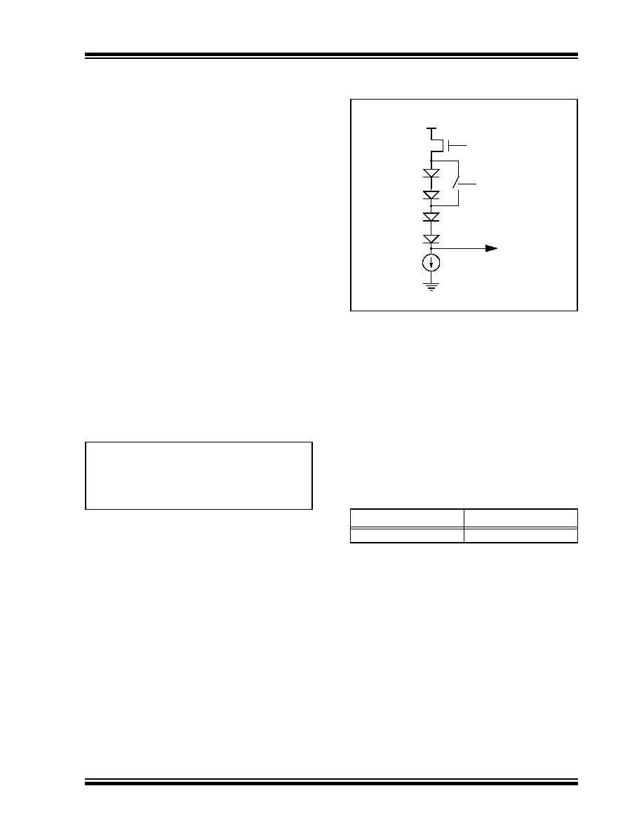
Circuit Operation
Figure 14-1 shows a simplified block diagram of the
temperature circuit. The proportional voltage output is
achieved by measuring the forward voltage drop across
multiple silicon junctions.
Equation 14-1 describes the output characteristics of
the temperature indicator.
EQUATION 14-1:
VOUT RANGES
The temperature sense circuit is integrated with the
Fixed
Voltage
Reference
(FVR)
module.
See
for
more information.
The circuit is enabled by setting the TSEN bit of the
FVRCON register. When disabled, the circuit draws no
current.
The circuit operates in either high or low range. The high
range, selected by setting the TSRNG bit of the
FVRCON register, provides a wider output voltage. This
provides more resolution over the temperature range,
but may be less consistent from part to part. This range
requires a higher bias voltage to operate and thus, a
higher VDD is needed.
The low range is selected by clearing the TSRNG bit of
the FVRCON0 register. The low range generates a
lower voltage drop and thus, a lower bias voltage is
needed to operate the circuit. The low range is provided
for low voltage operation.
FIGURE 14-1:
TEMPERATURE CIRCUIT
DIAGRAM
14.2
Minimum Operating VDD vs.
Minimum Sensing Temperature
When the temperature circuit is operated in low range,
the device may be operated at any operating voltage
that is within specifications.
When the temperature circuit is operated in high range,
the device operating voltage, VDD, must be high
enough to ensure that the temperature circuit is cor-
rectly biased.
range setting.
TABLE 14-1:
RECOMMENDED VDD VS.
RANGE
14.3
Temperature Output
The output of the circuit is measured using the internal
Analog-to-Digital Converter. A channel is reserved for
the temperature circuit output. Refer to Section 15.0
for
detailed information.
14.4
ADC Acquisition Time
To ensure accurate temperature measurements, the
user must wait at least 200
s after the ADC input
multiplexer is connected to the temperature indicator
output before the conversion is performed. In addition,
the user must wait 200
s between sequential
conversions of the temperature indicator output.
High Range: VOUT = VDD - 4VT
Low Range: VOUT = VDD - 2VT
Min. VDD, TSRNG = 1
Min. VDD, TSRNG = 0
3.6V
1.8V
TSEN
TSRNG
VDD
VOUT
To ADC
相关PDF资料 |
PDF描述 |
|---|---|
| PIC10F320T-I/OT | MCU 8BIT 448B FLASH SOT23-6 |
| PIC10F222T-I/OT | IC PIC MCU FLASH 512X12 SOT23-6 |
| PIC10F322-I/OT | IC MCU 8BIT 512B FLASH SOT23-6 |
| PIC10F220T-I/OT | IC PIC MCU FLASH 256X12 SOT23-6 |
| PIC10F206T-I/OT | IC PIC MCU FLASH 512X12 SOT23-6 |
相关代理商/技术参数 |
参数描述 |
|---|---|
| PIC10LF322 | 制造商:MICROCHIP 制造商全称:Microchip Technology 功能描述:6/8-Pin, High-Performance, Flash Microcontrollers |
| PIC10LF322-E/MC | 功能描述:8位微控制器 -MCU 896B FL 64B RAM 4I/O 8bit ADC 1.8-3.6V RoHS:否 制造商:Silicon Labs 核心:8051 处理器系列:C8051F39x 数据总线宽度:8 bit 最大时钟频率:50 MHz 程序存储器大小:16 KB 数据 RAM 大小:1 KB 片上 ADC:Yes 工作电源电压:1.8 V to 3.6 V 工作温度范围:- 40 C to + 105 C 封装 / 箱体:QFN-20 安装风格:SMD/SMT |
| PIC10LF322-E/OT | 功能描述:8位微控制器 -MCU 896B FL 64B RAM 4I/O 8bit ADC 1.8-3.6V RoHS:否 制造商:Silicon Labs 核心:8051 处理器系列:C8051F39x 数据总线宽度:8 bit 最大时钟频率:50 MHz 程序存储器大小:16 KB 数据 RAM 大小:1 KB 片上 ADC:Yes 工作电源电压:1.8 V to 3.6 V 工作温度范围:- 40 C to + 105 C 封装 / 箱体:QFN-20 安装风格:SMD/SMT |
| PIC10LF322-E/P | 功能描述:8位微控制器 -MCU 896B FL 64B RAM 4I/O 8bit ADC 1.8-3.6V RoHS:否 制造商:Silicon Labs 核心:8051 处理器系列:C8051F39x 数据总线宽度:8 bit 最大时钟频率:50 MHz 程序存储器大小:16 KB 数据 RAM 大小:1 KB 片上 ADC:Yes 工作电源电压:1.8 V to 3.6 V 工作温度范围:- 40 C to + 105 C 封装 / 箱体:QFN-20 安装风格:SMD/SMT |
| PIC10LF322-I/MC | 功能描述:8位微控制器 -MCU 896B FL 64B RAM 4I/O 8bit ADC 1.8-3.6V RoHS:否 制造商:Silicon Labs 核心:8051 处理器系列:C8051F39x 数据总线宽度:8 bit 最大时钟频率:50 MHz 程序存储器大小:16 KB 数据 RAM 大小:1 KB 片上 ADC:Yes 工作电源电压:1.8 V to 3.6 V 工作温度范围:- 40 C to + 105 C 封装 / 箱体:QFN-20 安装风格:SMD/SMT |
发布紧急采购,3分钟左右您将得到回复。