- 您现在的位置:买卖IC网 > PDF目录11404 > PIC16C55-XTI/SS (Microchip Technology)IC MCU OTP 512X12 28SSOP PDF资料下载
参数资料
| 型号: | PIC16C55-XTI/SS |
| 厂商: | Microchip Technology |
| 文件页数: | 126/194页 |
| 文件大小: | 0K |
| 描述: | IC MCU OTP 512X12 28SSOP |
| 产品培训模块: | Asynchronous Stimulus |
| 标准包装: | 47 |
| 系列: | PIC® 16C |
| 核心处理器: | PIC |
| 芯体尺寸: | 8-位 |
| 速度: | 4MHz |
| 外围设备: | POR,WDT |
| 输入/输出数: | 20 |
| 程序存储器容量: | 768B(512 x 12) |
| 程序存储器类型: | OTP |
| RAM 容量: | 24 x 8 |
| 电压 - 电源 (Vcc/Vdd): | 3 V ~ 6.25 V |
| 振荡器型: | 外部 |
| 工作温度: | -40°C ~ 85°C |
| 封装/外壳: | 28-SSOP(0.209",5.30mm 宽) |
| 包装: | 管件 |
| 配用: | 309-1026-ND - ADAPTER 28-SSOP TO 28-DIP |
第1页第2页第3页第4页第5页第6页第7页第8页第9页第10页第11页第12页第13页第14页第15页第16页第17页第18页第19页第20页第21页第22页第23页第24页第25页第26页第27页第28页第29页第30页第31页第32页第33页第34页第35页第36页第37页第38页第39页第40页第41页第42页第43页第44页第45页第46页第47页第48页第49页第50页第51页第52页第53页第54页第55页第56页第57页第58页第59页第60页第61页第62页第63页第64页第65页第66页第67页第68页第69页第70页第71页第72页第73页第74页第75页第76页第77页第78页第79页第80页第81页第82页第83页第84页第85页第86页第87页第88页第89页第90页第91页第92页第93页第94页第95页第96页第97页第98页第99页第100页第101页第102页第103页第104页第105页第106页第107页第108页第109页第110页第111页第112页第113页第114页第115页第116页第117页第118页第119页第120页第121页第122页第123页第124页第125页当前第126页第127页第128页第129页第130页第131页第132页第133页第134页第135页第136页第137页第138页第139页第140页第141页第142页第143页第144页第145页第146页第147页第148页第149页第150页第151页第152页第153页第154页第155页第156页第157页第158页第159页第160页第161页第162页第163页第164页第165页第166页第167页第168页第169页第170页第171页第172页第173页第174页第175页第176页第177页第178页第179页第180页第181页第182页第183页第184页第185页第186页第187页第188页第189页第190页第191页第192页第193页第194页
2002 Microchip Technology Inc.
Preliminary
DS30453D-page 35
PIC16C5X
7.0
I/O PORTS
As with any other register, the I/O Registers can be
written and read under program control. However, read
instructions (e.g., MOVF PORTB,W) always read the I/O
pins independent of the pin’s input/output modes. On
RESET, all I/O ports are defined as input (inputs are at
hi-impedance) since the I/O control registers (TRISA,
TRISB, TRISC) are all set.
7.1
PORTA
PORTA is a 4-bit I/O Register. Only the low order 4 bits
are used (RA<3:0>). Bits 7-4 are unimplemented and
read as '0's.
7.2
PORTB
PORTB is an 8-bit I/O Register (PORTB<7:0>).
7.3
PORTC
PORTC is an 8-bit I/O Register for PIC16C55,
PIC16C57 and PIC16CR57.
PORTC is a General Purpose Register for PIC16C54,
PIC16CR54, PIC16C56, PIC16CR56, PIC16C58 and
PIC16CR58.
7.4
TRIS Registers
The Output Driver Control Registers are loaded with
the contents of the W Register by executing the
TRIS f
instruction. A '1' from a TRIS Register bit puts
the corresponding output driver in a hi-impedance
(input) mode. A '0' puts the contents of the output data
latch on the selected pins, enabling the output buffer.
The TRIS Registers are “write-only” and are set (output
drivers disabled) upon RESET.
7.5
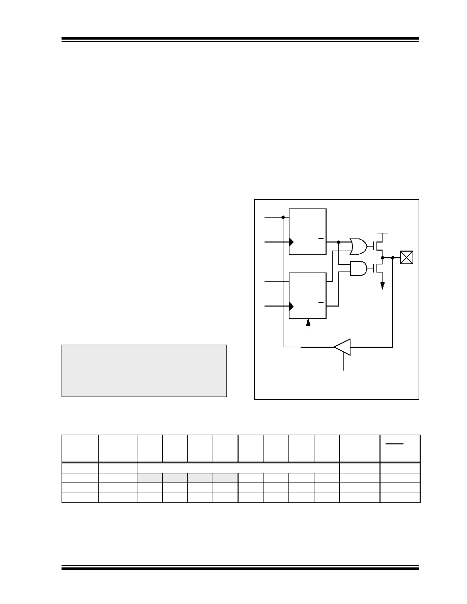
I/O Interfacing
The equivalent circuit for an I/O port pin is shown in
Figure 7-1. All ports may be used for both input and
output operation. For input operations these ports are
non-latching. Any input must be present until read by
an input instruction (e.g., MOVF PORTB, W). The out-
puts are latched and remain unchanged until the output
latch is rewritten. To use a port pin as output, the corre-
sponding direction control bit (in TRISA, TRISB,
TRISC) must be cleared (= 0). For use as an input, the
corresponding TRIS bit must be set. Any I/O pin can be
programmed individually as input or output.
FIGURE 7-1:
EQUIVALENT CIRCUIT
FOR A SINGLE I/O PIN
TABLE 7-1:
SUMMARY OF PORT REGISTERS
Note:
A read of the ports reads the pins, not the
output data latches. That is, if an output
driver on a pin is enabled and driven high,
but the external system is holding it low, a
read of the port will indicate that the pin is
low.
Note 1: I/O pins have protection diodes to VDD and VSS.
Data
Bus
Q
D
Q
CK
Q
D
Q
CK
P
N
WR
Port
TRIS ‘f’
Data
TRIS
RD Port
VSS
VDD
I/O
pin(1)
W
Reg
Latch
RESET
Address
Name
Bit 7
Bit 6
Bit 5
Bit 4
Bit 3
Bit 2
Bit 1
Bit 0
Value on
Power-On
Reset
Value on
MCLR and
WDT Reset
N/A
TRIS
I/O Control Registers (TRISA, TRISB, TRISC)
1111 1111
05h
PORTA
—
RA3
RA2
RA1
RA0
---- xxxx
---- uuuu
06h
PORTB
RB7
RB6
RB5
RB4
RB3
RB2
RB1
RB0
xxxx xxxx
uuuu uuuu
07h
PORTC
RC7
RC6
RC5
RC4
RC3
RC2
RC1
RC0
xxxx xxxx
uuuu uuuu
Legend: x = unknown, u = unchanged, — = unimplemented, read as '0', Shaded cells = unimplemented, read as ‘0’
相关PDF资料 |
PDF描述 |
|---|---|
| GRM2196T2A3R5CD01D | CAP CER 3.5PF 100V T2H 0805 |
| GRM2196T2A3R1CD01D | CAP CER 3.1PF 100V T2H 0805 |
| GRM2196T2A2R8CD01D | CAP CER 2.8PF 100V T2H 0805 |
| GRM2196T2A2R6CD01D | CAP CER 2.6PF 100V T2H 0805 |
| PIC18F8393T-I/PT | IC PIC MCU FLASH 4KX16 80TQFP |
相关代理商/技术参数 |
参数描述 |
|---|---|
| PIC16C56/JW | 功能描述:8位微控制器 -MCU 1.5KB 25 RAM 12 I/O RoHS:否 制造商:Silicon Labs 核心:8051 处理器系列:C8051F39x 数据总线宽度:8 bit 最大时钟频率:50 MHz 程序存储器大小:16 KB 数据 RAM 大小:1 KB 片上 ADC:Yes 工作电源电压:1.8 V to 3.6 V 工作温度范围:- 40 C to + 105 C 封装 / 箱体:QFN-20 安装风格:SMD/SMT |
| PIC16C56-10/P | 功能描述:8位微控制器 -MCU 1.5KB 25 RAM 12 I/O 10 MHz PDIP18 RoHS:否 制造商:Silicon Labs 核心:8051 处理器系列:C8051F39x 数据总线宽度:8 bit 最大时钟频率:50 MHz 程序存储器大小:16 KB 数据 RAM 大小:1 KB 片上 ADC:Yes 工作电源电压:1.8 V to 3.6 V 工作温度范围:- 40 C to + 105 C 封装 / 箱体:QFN-20 安装风格:SMD/SMT |
| PIC16C56-10/SO | 功能描述:8位微控制器 -MCU 1.5KB 25 RAM 12 I/O 10 MHz SOIC18 RoHS:否 制造商:Silicon Labs 核心:8051 处理器系列:C8051F39x 数据总线宽度:8 bit 最大时钟频率:50 MHz 程序存储器大小:16 KB 数据 RAM 大小:1 KB 片上 ADC:Yes 工作电源电压:1.8 V to 3.6 V 工作温度范围:- 40 C to + 105 C 封装 / 箱体:QFN-20 安装风格:SMD/SMT |
| PIC16C56-10/SS | 功能描述:8位微控制器 -MCU 1.5KB 25 RAM 12 I/O 10 MHz SSOP20 RoHS:否 制造商:Silicon Labs 核心:8051 处理器系列:C8051F39x 数据总线宽度:8 bit 最大时钟频率:50 MHz 程序存储器大小:16 KB 数据 RAM 大小:1 KB 片上 ADC:Yes 工作电源电压:1.8 V to 3.6 V 工作温度范围:- 40 C to + 105 C 封装 / 箱体:QFN-20 安装风格:SMD/SMT |
| PIC16C56-10E/P | 功能描述:8位微控制器 -MCU 1.5KB 25 RAM 12 I/O RoHS:否 制造商:Silicon Labs 核心:8051 处理器系列:C8051F39x 数据总线宽度:8 bit 最大时钟频率:50 MHz 程序存储器大小:16 KB 数据 RAM 大小:1 KB 片上 ADC:Yes 工作电源电压:1.8 V to 3.6 V 工作温度范围:- 40 C to + 105 C 封装 / 箱体:QFN-20 安装风格:SMD/SMT |
发布紧急采购,3分钟左右您将得到回复。