- 您现在的位置:买卖IC网 > PDF目录11461 > PIC16C711-20I/SS (Microchip Technology)IC MCU OTP 1KX14 A/D 20SSOP PDF资料下载
参数资料
| 型号: | PIC16C711-20I/SS |
| 厂商: | Microchip Technology |
| 文件页数: | 40/177页 |
| 文件大小: | 0K |
| 描述: | IC MCU OTP 1KX14 A/D 20SSOP |
| 产品培训模块: | Asynchronous Stimulus |
| 标准包装: | 67 |
| 系列: | PIC® 16C |
| 核心处理器: | PIC |
| 芯体尺寸: | 8-位 |
| 速度: | 20MHz |
| 外围设备: | 欠压检测/复位,POR,WDT |
| 输入/输出数: | 13 |
| 程序存储器容量: | 1.75KB(1K x 14) |
| 程序存储器类型: | OTP |
| RAM 容量: | 68 x 8 |
| 电压 - 电源 (Vcc/Vdd): | 4 V ~ 6 V |
| 数据转换器: | A/D 4x8b |
| 振荡器型: | 外部 |
| 工作温度: | -40°C ~ 85°C |
| 封装/外壳: | 20-SSOP(0.209",5.30mm 宽) |
| 包装: | 管件 |
| 配用: | 309-1016-ND - ADAPTER 20-SSOP TO 18-DIP |
第1页第2页第3页第4页第5页第6页第7页第8页第9页第10页第11页第12页第13页第14页第15页第16页第17页第18页第19页第20页第21页第22页第23页第24页第25页第26页第27页第28页第29页第30页第31页第32页第33页第34页第35页第36页第37页第38页第39页当前第40页第41页第42页第43页第44页第45页第46页第47页第48页第49页第50页第51页第52页第53页第54页第55页第56页第57页第58页第59页第60页第61页第62页第63页第64页第65页第66页第67页第68页第69页第70页第71页第72页第73页第74页第75页第76页第77页第78页第79页第80页第81页第82页第83页第84页第85页第86页第87页第88页第89页第90页第91页第92页第93页第94页第95页第96页第97页第98页第99页第100页第101页第102页第103页第104页第105页第106页第107页第108页第109页第110页第111页第112页第113页第114页第115页第116页第117页第118页第119页第120页第121页第122页第123页第124页第125页第126页第127页第128页第129页第130页第131页第132页第133页第134页第135页第136页第137页第138页第139页第140页第141页第142页第143页第144页第145页第146页第147页第148页第149页第150页第151页第152页第153页第154页第155页第156页第157页第158页第159页第160页第161页第162页第163页第164页第165页第166页第167页第168页第169页第170页第171页第172页第173页第174页第175页第176页第177页
134
7593L–AVR–09/12
AT90USB64/128
Using the ICRn Register for defining TOP works well when using fixed TOP values. By using
ICRn, the OCRnA Register is free to be used for generating a PWM output on OCnA. However,
if the base PWM frequency is actively changed by changing the TOP value, using the OCRnA as
TOP is clearly a better choice due to its double buffer feature.
In phase and frequency correct PWM mode, the compare units allow generation of PWM wave-
forms on the OCnx pins. Setting the COMnx1:0 bits to two will produce a non-inverted PWM and
an inverted PWM output can be generated by setting the COMnx1:0 to three (see Table 15-3 on
page 138). The actual OCnx value will only be visible on the port pin if the data direction for the
port pin is set as output (DDR_OCnx). The PWM waveform is generated by setting (or clearing)
the OCnx Register at the compare match between OCRnx and TCNTn when the counter incre-
ments, and clearing (or setting) the OCnx Register at compare match between OCRnx and
TCNTn when the counter decrements. The PWM frequency for the output when using phase
and frequency correct PWM can be calculated by the following equation:
The N variable represents the prescaler divider (1, 8, 64, 256, or 1024).
The extreme values for the OCRnx Register represents special cases when generating a PWM
waveform output in the phase correct PWM mode. If the OCRnx is set equal to BOTTOM the
output will be continuously low and if set equal to TOP the output will be set to high for non-
inverted PWM mode. For inverted PWM the output will have the opposite logic values. If OCR1A
is used to define the TOP value (WGM13:0 = 9) and COM1A1:0 = 1, the OC1A output will toggle
with a 50% duty cycle.
15.9
Timer/Counter timing diagrams
The Timer/Counter is a synchronous design and the timer clock (clk
Tn) is therefore shown as a
clock enable signal in the following figures. The figures include information on when Interrupt
Flags are set, and when the OCRnx Register is updated with the OCRnx buffer value (only for
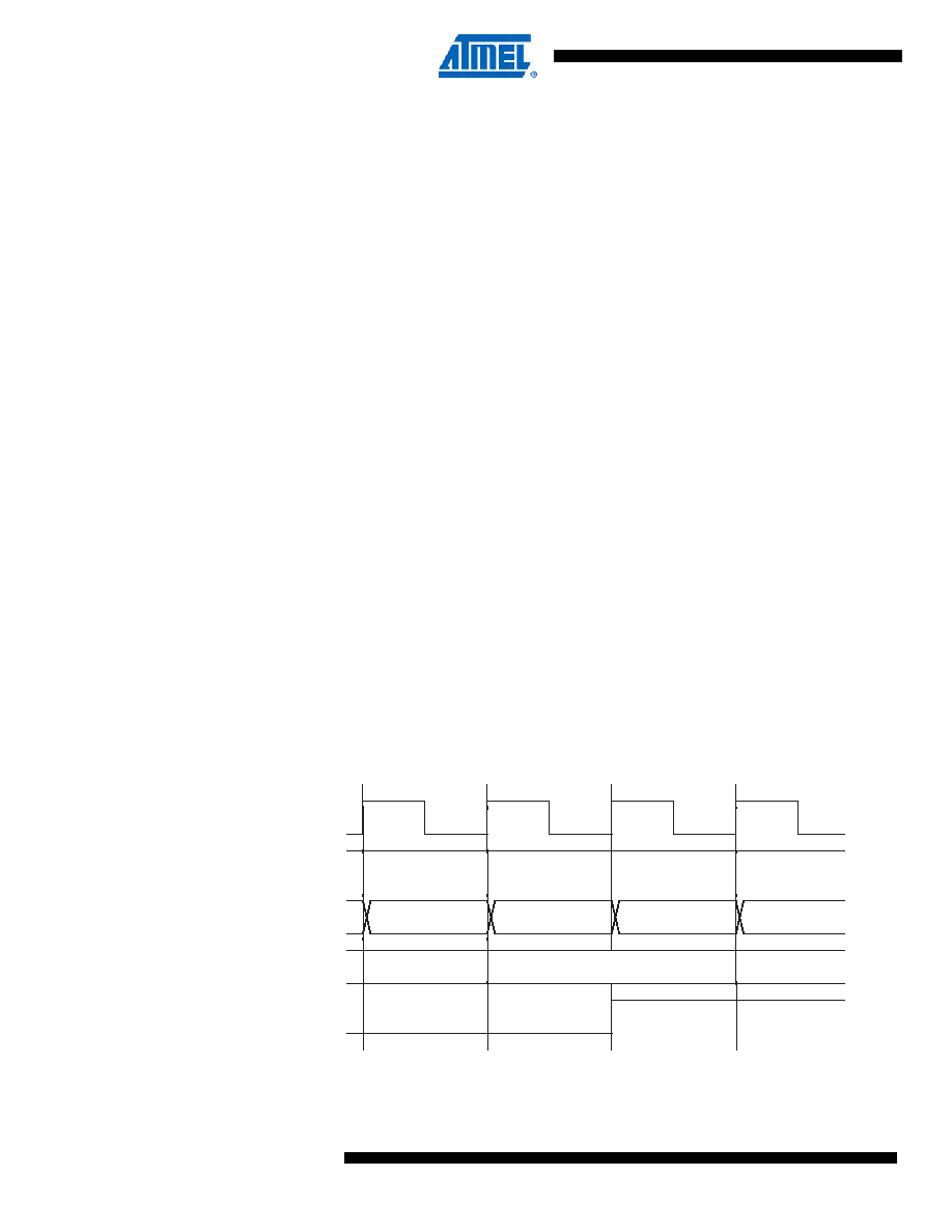
modes utilizing double buffering). Figure 15-10 shows a timing diagram for the setting of OCFnx.
Figure 15-10. Timer/Counter timing diagram, setting of OCFnx, no prescaling.
Figure 15-11 on page 135 shows the same timing data, but with the prescaler enabled.
fOCnxPFCPWM
f
clk_I/O
2
NTOP
----------------------------
=
clk
Tn
(clk
I/O/1)
OCFnx
clk
I/O
OCRnx
TCNTn
OCRnx value
OCRnx - 1
OCRnx
OCRnx + 1
OCRnx + 2
相关PDF资料 |
PDF描述 |
|---|---|
| GRM319R61C105KAA3D | CAP CER 1UF 16V 10% X5R 1206 |
| GRM2196R1H201JZ01D | CAP CER 200PF 50V 5% R2H 0805 |
| PIC16LC715-04/SS | IC MCU OTP 2KX14 A/D PWM 20SSOP |
| VI-J2Z-IY-B1 | CONVERTER MOD DC/DC 2V 20W |
| PIC16C715T-04/SS | IC MCU OTP 2KX14 A/D 20SSOP |
相关代理商/技术参数 |
参数描述 |
|---|---|
| PIC16C711-20P | 制造商:Microchip Technology Inc 功能描述:IC PIC16C711-20P S40004-RL4 ((NS)) |
| PIC16C711T-04/SO | 功能描述:8位微控制器 -MCU 1.75KB 68 RAM 13 I/O 4MHz SOIC18 RoHS:否 制造商:Silicon Labs 核心:8051 处理器系列:C8051F39x 数据总线宽度:8 bit 最大时钟频率:50 MHz 程序存储器大小:16 KB 数据 RAM 大小:1 KB 片上 ADC:Yes 工作电源电压:1.8 V to 3.6 V 工作温度范围:- 40 C to + 105 C 封装 / 箱体:QFN-20 安装风格:SMD/SMT |
| PIC16C711T-04/SS | 功能描述:8位微控制器 -MCU 1.75KB 68 RAM 13 I/O 4MHz SSOP20 RoHS:否 制造商:Silicon Labs 核心:8051 处理器系列:C8051F39x 数据总线宽度:8 bit 最大时钟频率:50 MHz 程序存储器大小:16 KB 数据 RAM 大小:1 KB 片上 ADC:Yes 工作电源电压:1.8 V to 3.6 V 工作温度范围:- 40 C to + 105 C 封装 / 箱体:QFN-20 安装风格:SMD/SMT |
| PIC16C711T-04E/SO | 功能描述:8位微控制器 -MCU 1.75KB 68 RAM 13 I/O 4MHz Ext Temp SOIC18 RoHS:否 制造商:Silicon Labs 核心:8051 处理器系列:C8051F39x 数据总线宽度:8 bit 最大时钟频率:50 MHz 程序存储器大小:16 KB 数据 RAM 大小:1 KB 片上 ADC:Yes 工作电源电压:1.8 V to 3.6 V 工作温度范围:- 40 C to + 105 C 封装 / 箱体:QFN-20 安装风格:SMD/SMT |
| PIC16C711T-04E/SS | 功能描述:8位微控制器 -MCU 1.75KB 68 RAM 13 I/O RoHS:否 制造商:Silicon Labs 核心:8051 处理器系列:C8051F39x 数据总线宽度:8 bit 最大时钟频率:50 MHz 程序存储器大小:16 KB 数据 RAM 大小:1 KB 片上 ADC:Yes 工作电源电压:1.8 V to 3.6 V 工作温度范围:- 40 C to + 105 C 封装 / 箱体:QFN-20 安装风格:SMD/SMT |
发布紧急采购,3分钟左右您将得到回复。