- 您现在的位置:买卖IC网 > PDF目录10864 > PIC16C923T-08I/PT (Microchip Technology)IC MCU OTP 4KX14 LCD DVR 64TQFP PDF资料下载
参数资料
| 型号: | PIC16C923T-08I/PT |
| 厂商: | Microchip Technology |
| 文件页数: | 88/115页 |
| 文件大小: | 0K |
| 描述: | IC MCU OTP 4KX14 LCD DVR 64TQFP |
| 标准包装: | 1,200 |
| 系列: | PIC® 16C |
| 核心处理器: | PIC |
| 芯体尺寸: | 8-位 |
| 速度: | 8MHz |
| 连通性: | I²C,SPI |
| 外围设备: | LCD,POR,PWM,WDT |
| 输入/输出数: | 25 |
| 程序存储器容量: | 7KB(4K x 14) |
| 程序存储器类型: | OTP |
| RAM 容量: | 176 x 8 |
| 电压 - 电源 (Vcc/Vdd): | 4 V ~ 6 V |
| 振荡器型: | 外部 |
| 工作温度: | -40°C ~ 85°C |
| 封装/外壳: | 64-TQFP |
| 包装: | 带卷 (TR) |
| 配用: | DVA16PQ640-ND - ADAPTER DEVICE FOR MPLAB-ICE AC164023-ND - MODULE SKT PROMATEII 68TQFP |
第1页第2页第3页第4页第5页第6页第7页第8页第9页第10页第11页第12页第13页第14页第15页第16页第17页第18页第19页第20页第21页第22页第23页第24页第25页第26页第27页第28页第29页第30页第31页第32页第33页第34页第35页第36页第37页第38页第39页第40页第41页第42页第43页第44页第45页第46页第47页第48页第49页第50页第51页第52页第53页第54页第55页第56页第57页第58页第59页第60页第61页第62页第63页第64页第65页第66页第67页第68页第69页第70页第71页第72页第73页第74页第75页第76页第77页第78页第79页第80页第81页第82页第83页第84页第85页第86页第87页当前第88页第89页第90页第91页第92页第93页第94页第95页第96页第97页第98页第99页第100页第101页第102页第103页第104页第105页第106页第107页第108页第109页第110页第111页第112页第113页第114页第115页
PIC16C9XX
DS30444E - page 74
1997 Microchip Technology Inc.
11.3.1
SLAVE MODE
In slave mode, the SCL and SDA pins must be cong-
ured as inputs (TRISC<4:3> set). The SSP module will
override the input state with the output data when
required (slave-transmitter).
When an address is matched or the data transfer after
an address match is received, the hardware automati-
cally will generate the acknowledge (ACK) pulse, and
then load the SSPBUF register with the received value
currently in the SSPSR register.
There are certain conditions that will cause the SSP
module not to give this ACK pulse. These are if either
(or both):
a)
The buffer full bit BF (SSPSTAT<0>) was set
before the transfer was received.
b)
The overow bit SSPOV (SSPCON<6>) was set
before the transfer was received.
In this case, the SSPSR register value is not loaded into
the SSPBUF, but bit SSPIF (PIR1<3>) is set. Table 11-3
shows what happens when a data transfer byte is
received, given the status of bits BF and SSPOV. The
shaded cells show the condition where user software
did not properly clear the overow condition. Flag bit BF
is cleared by reading the SSPBUF register while bit
SSPOV is cleared through software.
The SCL clock input must have a minimum high and
low time for proper operation. The high and low times of
the I2C specication as well as the requirement of the
SSP module is shown in timing parameter #100 and
parameter #101.
11.3.1.1
ADDRESSING
Once the SSP module has been enabled, it waits for a
START condition to occur. Following the START condi-
tion, the 8-bits are shifted into the SSPSR register. All
incoming bits are sampled with the rising edge of the
clock (SCL) line. The value of register SSPSR<7:1> is
compared to the value of the SSPADD register. The
address is compared on the falling edge of the eighth
clock (SCL) pulse. If the addresses match, and the BF
and SSPOV bits are clear, the following events occur:
a)
The SSPSR register value is loaded into the
SSPBUF register.
b)
The buffer full bit, BF is set.
c)
An ACK pulse is generated.
d)
SSP interrupt ag bit, SSPIF (PIR1<3>) is set
(interrupt is generated if enabled) - on the falling
edge of the ninth SCL pulse.
In 10-bit address mode, two address bytes need to be
received by the slave (Figure 11-10). The ve Most Sig-
nicant bits (MSbs) of the rst address byte specify if
this is a 10-bit address. Bit R/W (SSPSTAT<2>) must
specify a write so the slave device will receive the sec-
ond address byte. For a 10-bit address the rst byte
would equal ‘1111 0 A9 A8 0’, where A9 and A8 are
the two MSbs of the address. The sequence of events
for a 10-bit address is as follows, with steps 7- 9 for
slave-transmitter:
1.
Receive rst (high) byte of Address (bits SSPIF,
BF, and bit UA (SSPSTAT<1>) are set).
2.
Update the SSPADD register with second (low)
byte of Address (clears bit UA and releases the
SCL line).
3.
Read the SSPBUF register (clears bit BF) and
clear ag bit SSPIF.
4.
Receive second (low) byte of Address (bits
SSPIF, BF, and UA are set).
5.
Update the SSPADD register with the rst (high)
byte of Address, if match releases SCL line, this
will clear bit UA.
6.
Read the SSPBUF register (clears bit BF) and
clear ag bit SSPIF.
7.
Receive repeated START condition.
8.
Receive rst (high) byte of Address (bits SSPIF
and BF are set).
9.
Read the SSPBUF register (clears bit BF) and
clear ag bit SSPIF.
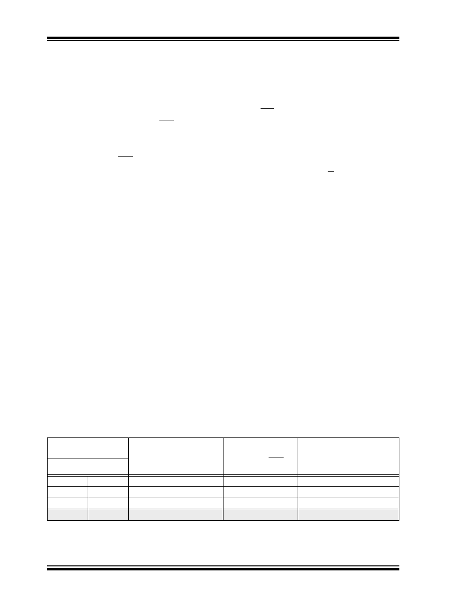
TABLE 11-3: DATA TRANSFER RECEIVED BYTE ACTIONS
Status Bits as Data
Transfer is Received
SSPSR
→ SSPBUF
Generate ACK
Pulse
Set bit SSPIF
(SSP Interrupt occurs
if enabled)
BF
SSPOV
0
Yes
1
0
No
Yes
1
No
Yes
0
1
No
Yes
相关PDF资料 |
PDF描述 |
|---|---|
| VI-25L-IW-S | CONVERTER MOD DC/DC 28V 100W |
| PIC16C923T-08I/L | IC MCU OTP 4KX14 LCD DVR 68PLCC |
| VI-25L-CU-F3 | CONVERTER MOD DC/DC 28V 200W |
| PIC16C923T-04/PT | IC MCU OTP 4KX14 LCD DVR 64TQFP |
| VI-25L-CU-F2 | CONVERTER MOD DC/DC 28V 200W |
相关代理商/技术参数 |
参数描述 |
|---|---|
| PIC16C924/CL | 功能描述:8位微控制器 -MCU 7KB 176 RAM 52 I/O RoHS:否 制造商:Silicon Labs 核心:8051 处理器系列:C8051F39x 数据总线宽度:8 bit 最大时钟频率:50 MHz 程序存储器大小:16 KB 数据 RAM 大小:1 KB 片上 ADC:Yes 工作电源电压:1.8 V to 3.6 V 工作温度范围:- 40 C to + 105 C 封装 / 箱体:QFN-20 安装风格:SMD/SMT |
| PIC16C924-04/L | 功能描述:8位微控制器 -MCU 7KB 176 RAM 52 I/O RoHS:否 制造商:Silicon Labs 核心:8051 处理器系列:C8051F39x 数据总线宽度:8 bit 最大时钟频率:50 MHz 程序存储器大小:16 KB 数据 RAM 大小:1 KB 片上 ADC:Yes 工作电源电压:1.8 V to 3.6 V 工作温度范围:- 40 C to + 105 C 封装 / 箱体:QFN-20 安装风格:SMD/SMT |
| PIC16C924-04/PT | 功能描述:8位微控制器 -MCU 7KB 176 RAM 52 I/O RoHS:否 制造商:Silicon Labs 核心:8051 处理器系列:C8051F39x 数据总线宽度:8 bit 最大时钟频率:50 MHz 程序存储器大小:16 KB 数据 RAM 大小:1 KB 片上 ADC:Yes 工作电源电压:1.8 V to 3.6 V 工作温度范围:- 40 C to + 105 C 封装 / 箱体:QFN-20 安装风格:SMD/SMT |
| PIC16C924-04I/L | 功能描述:8位微控制器 -MCU 7KB 176 RAM 52 I/O RoHS:否 制造商:Silicon Labs 核心:8051 处理器系列:C8051F39x 数据总线宽度:8 bit 最大时钟频率:50 MHz 程序存储器大小:16 KB 数据 RAM 大小:1 KB 片上 ADC:Yes 工作电源电压:1.8 V to 3.6 V 工作温度范围:- 40 C to + 105 C 封装 / 箱体:QFN-20 安装风格:SMD/SMT |
| PIC16C924-04I/PT | 功能描述:8位微控制器 -MCU 7KB 176 RAM 52 I/O RoHS:否 制造商:Silicon Labs 核心:8051 处理器系列:C8051F39x 数据总线宽度:8 bit 最大时钟频率:50 MHz 程序存储器大小:16 KB 数据 RAM 大小:1 KB 片上 ADC:Yes 工作电源电压:1.8 V to 3.6 V 工作温度范围:- 40 C to + 105 C 封装 / 箱体:QFN-20 安装风格:SMD/SMT |
发布紧急采购,3分钟左右您将得到回复。