- 您现在的位置:买卖IC网 > PDF目录11481 > PIC16CE625T-04/SO (Microchip Technology)IC MCU OTP 2KX14 EE COMP 18SOIC PDF资料下载
参数资料
| 型号: | PIC16CE625T-04/SO |
| 厂商: | Microchip Technology |
| 文件页数: | 55/100页 |
| 文件大小: | 0K |
| 描述: | IC MCU OTP 2KX14 EE COMP 18SOIC |
| 产品培训模块: | Asynchronous Stimulus |
| 标准包装: | 1,100 |
| 系列: | PIC® 16C |
| 核心处理器: | PIC |
| 芯体尺寸: | 8-位 |
| 速度: | 4MHz |
| 外围设备: | 欠压检测/复位,POR,WDT |
| 输入/输出数: | 13 |
| 程序存储器容量: | 3.5KB(2K x 14) |
| 程序存储器类型: | OTP |
| EEPROM 大小: | 128 x 8 |
| RAM 容量: | 128 x 8 |
| 电压 - 电源 (Vcc/Vdd): | 3 V ~ 5.5 V |
| 振荡器型: | 外部 |
| 工作温度: | 0°C ~ 70°C |
| 封装/外壳: | 18-SOIC(0.295",7.50mm 宽) |
| 包装: | 带卷 (TR) |
第1页第2页第3页第4页第5页第6页第7页第8页第9页第10页第11页第12页第13页第14页第15页第16页第17页第18页第19页第20页第21页第22页第23页第24页第25页第26页第27页第28页第29页第30页第31页第32页第33页第34页第35页第36页第37页第38页第39页第40页第41页第42页第43页第44页第45页第46页第47页第48页第49页第50页第51页第52页第53页第54页当前第55页第56页第57页第58页第59页第60页第61页第62页第63页第64页第65页第66页第67页第68页第69页第70页第71页第72页第73页第74页第75页第76页第77页第78页第79页第80页第81页第82页第83页第84页第85页第86页第87页第88页第89页第90页第91页第92页第93页第94页第95页第96页第97页第98页第99页第100页
PIC16CE62X
DS40182C-page 48
1999 Microchip Technology Inc.
EXAMPLE 9-1:
VOLTAGE REFERENCE
CONFIGURATION
9.2
Voltage Reference Accuracy/Error
The full range of VSS to VDD cannot be realized due to
the construction of the module. The transistors on the
top and bottom of the resistor ladder network
The Voltage Reference is VDD derived and therefore,
the VREF output changes with fluctuations in VDD. The
absolute accuracy of the Voltage Reference can be
found in Table 13-2.
9.3
Operation During Sleep
When the device wakes up from sleep through an
interrupt or a Watchdog Timer time-out, the contents of
the VRCON register are not affected. To minimize
current consumption in SLEEP mode, the Voltage
Reference should be disabled.
MOVLW
0x02
; 4 Inputs Muxed
MOVWF
CMCON
; to 2 comps.
BSF
STATUS,RP0
; go to Bank 1
MOVLW
0x07
; RA3-RA0 are
MOVWF
TRISA
; outputs
MOVLW
0xA6
; enable VREF
MOVWF
VRCON
; low range
; set VR<3:0>=6
BCF
STATUS,RP0
; go to Bank 0
CALL
DELAY10
; 10
s delay
9.4
Effects of a Reset
A device reset disables the Voltage Reference by clear-
ing bit VREN (VRCON<7>). This reset also disconnects
the reference from the RA2 pin by clearing bit VROE
(VRCON<6>) and selects the high voltage range by
clearing bit VRR (VRCON<5>). The VREF value select
bits, VRCON<3:0>, are also cleared.
9.5
Connection Considerations
The
Voltage
Reference
Module
operates
independently of the comparator module. The output of
the reference generator may be connected to the RA2
pin if the TRISA<2> bit is set and the VROE bit,
VRCON<6>, is set. Enabling the Voltage Reference
output onto the RA2 pin with an input signal present will
increase current consumption. Connecting RA2 as a
digital
output with VREF enabled will also increase
current consumption.
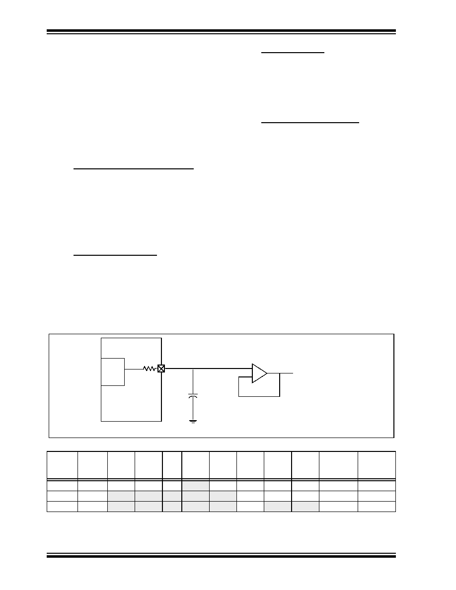
The RA2 pin can be used as a simple D/A output with
limited drive capability. Due to the limited drive
capability, a buffer must be used in conjunction with the
Voltage Reference output for external connections to
VREF.
shows
an
example
buffering
technique.
FIGURE 9-2:
VOLTAGE REFERENCE OUTPUT BUFFER EXAMPLE
TABLE 9-1:
REGISTERS ASSOCIATED WITH VOLTAGE REFERENCE
Legend: - = Unimplemented, read as "0"
Address
Name
Bit 7
Bit 6
Bit 5
Bit 4
Bit 3
Bit 2
Bit 1
Bit 0
Value On
POR / BOD
Value On
All Other
Resets
9Fh
VRCON
VREN
VROE
VRR
—VR3
VR2
VR1
VR0
000- 0000
1Fh
CMCON
C2OUT
C1OUT
—
CIS
CM2
CM1
CM0
00-- 0000
85h
TRISA
—
TRISA4
TRISA3
TRISA2
TRISA1
TRISA0
---1 1111
VREF Output
+
–
VREF
Module
Voltage
Reference
Output
Impedance
R
(1)
RA2
Note 1:
R is dependent upon the Voltage Reference Configuration VRCON<3:0> and VRCON<5>.
相关PDF资料 |
PDF描述 |
|---|---|
| ADG508FBNZ | IC MULTIPLEXER 8X1 16DIP |
| VI-B2Z-IX-B1 | CONVERTER MOD DC/DC 2V 30W |
| PIC16F946T-I/PT | IC PIC MCU FLASH 8KX14 64TQFP |
| ADG1434YRUZ | IC SWITCH QUAD SPDT 20TSSOP |
| DSPIC33FJ12MC202T-I/SS | IC DSPIC MCU/DSP 12K 28SSOP |
相关代理商/技术参数 |
参数描述 |
|---|---|
| PIC16CE625T-20/SO | 功能描述:8位微控制器 -MCU 3.5KB 128 RAM 13 I/O RoHS:否 制造商:Silicon Labs 核心:8051 处理器系列:C8051F39x 数据总线宽度:8 bit 最大时钟频率:50 MHz 程序存储器大小:16 KB 数据 RAM 大小:1 KB 片上 ADC:Yes 工作电源电压:1.8 V to 3.6 V 工作温度范围:- 40 C to + 105 C 封装 / 箱体:QFN-20 安装风格:SMD/SMT |
| PIC16CE625T-20/SS | 功能描述:8位微控制器 -MCU 3.5KB 128 RAM 13 I/O RoHS:否 制造商:Silicon Labs 核心:8051 处理器系列:C8051F39x 数据总线宽度:8 bit 最大时钟频率:50 MHz 程序存储器大小:16 KB 数据 RAM 大小:1 KB 片上 ADC:Yes 工作电源电压:1.8 V to 3.6 V 工作温度范围:- 40 C to + 105 C 封装 / 箱体:QFN-20 安装风格:SMD/SMT |
| PIC16CE625T-20E/SO | 功能描述:8位微控制器 -MCU 3.5KB 128 RAM 13 I/O RoHS:否 制造商:Silicon Labs 核心:8051 处理器系列:C8051F39x 数据总线宽度:8 bit 最大时钟频率:50 MHz 程序存储器大小:16 KB 数据 RAM 大小:1 KB 片上 ADC:Yes 工作电源电压:1.8 V to 3.6 V 工作温度范围:- 40 C to + 105 C 封装 / 箱体:QFN-20 安装风格:SMD/SMT |
| PIC16CE625T-20E/SS | 功能描述:8位微控制器 -MCU 3.5KB 128 RAM 13 I/O RoHS:否 制造商:Silicon Labs 核心:8051 处理器系列:C8051F39x 数据总线宽度:8 bit 最大时钟频率:50 MHz 程序存储器大小:16 KB 数据 RAM 大小:1 KB 片上 ADC:Yes 工作电源电压:1.8 V to 3.6 V 工作温度范围:- 40 C to + 105 C 封装 / 箱体:QFN-20 安装风格:SMD/SMT |
| PIC16CE625T-20I/SO | 功能描述:8位微控制器 -MCU 3.5KB 128 RAM 13 I/O RoHS:否 制造商:Silicon Labs 核心:8051 处理器系列:C8051F39x 数据总线宽度:8 bit 最大时钟频率:50 MHz 程序存储器大小:16 KB 数据 RAM 大小:1 KB 片上 ADC:Yes 工作电源电压:1.8 V to 3.6 V 工作温度范围:- 40 C to + 105 C 封装 / 箱体:QFN-20 安装风格:SMD/SMT |
发布紧急采购,3分钟左右您将得到回复。