- 您现在的位置:买卖IC网 > PDF目录11481 > PIC16CE625T-04/SO (Microchip Technology)IC MCU OTP 2KX14 EE COMP 18SOIC PDF资料下载
参数资料
| 型号: | PIC16CE625T-04/SO |
| 厂商: | Microchip Technology |
| 文件页数: | 72/100页 |
| 文件大小: | 0K |
| 描述: | IC MCU OTP 2KX14 EE COMP 18SOIC |
| 产品培训模块: | Asynchronous Stimulus |
| 标准包装: | 1,100 |
| 系列: | PIC® 16C |
| 核心处理器: | PIC |
| 芯体尺寸: | 8-位 |
| 速度: | 4MHz |
| 外围设备: | 欠压检测/复位,POR,WDT |
| 输入/输出数: | 13 |
| 程序存储器容量: | 3.5KB(2K x 14) |
| 程序存储器类型: | OTP |
| EEPROM 大小: | 128 x 8 |
| RAM 容量: | 128 x 8 |
| 电压 - 电源 (Vcc/Vdd): | 3 V ~ 5.5 V |
| 振荡器型: | 外部 |
| 工作温度: | 0°C ~ 70°C |
| 封装/外壳: | 18-SOIC(0.295",7.50mm 宽) |
| 包装: | 带卷 (TR) |
第1页第2页第3页第4页第5页第6页第7页第8页第9页第10页第11页第12页第13页第14页第15页第16页第17页第18页第19页第20页第21页第22页第23页第24页第25页第26页第27页第28页第29页第30页第31页第32页第33页第34页第35页第36页第37页第38页第39页第40页第41页第42页第43页第44页第45页第46页第47页第48页第49页第50页第51页第52页第53页第54页第55页第56页第57页第58页第59页第60页第61页第62页第63页第64页第65页第66页第67页第68页第69页第70页第71页当前第72页第73页第74页第75页第76页第77页第78页第79页第80页第81页第82页第83页第84页第85页第86页第87页第88页第89页第90页第91页第92页第93页第94页第95页第96页第97页第98页第99页第100页
1999 Microchip Technology Inc.
DS40182C-page 63
PIC16CE62X
10.8
Power-Down Mode (SLEEP)
The Power-down mode is entered by executing a
SLEEP
instruction.
If enabled, the Watchdog Timer will be cleared but
keeps running, the PD bit in the STATUS register is
cleared, the TO bit is set and the oscillator driver is
turned off. The I/O ports maintain the status they had
before SLEEP was executed (driving high, low, or
hi-impedance).
For lowest current consumption in this mode, all I/O
pins should be either at VDD or VSS, with no external
circuitry drawing current from the I/O pin, and the com-
parators and VREF should be disabled. I/O pins that are
hi-impedance inputs should be pulled high or low exter-
nally to avoid switching currents caused by floating
inputs. The T0CKI input should also be at VDD or VSS
for lowest current consumption. The contribution from
on chip pull-ups on PORTB should be considered.
The MCLR pin must be at a logic high level (VIHMC).
10.8.1
WAKE-UP FROM SLEEP
The device can wake-up from SLEEP through one of
the following events:
1.
External reset input on MCLR pin
2.
Watchdog Timer Wake-up (if WDT was enabled)
3.
Interrupt from RB0/INT pin, RB Port change, or
the Peripheral Interrupt (Comparator).
The first event will cause a device reset. The two latter
events are considered a continuation of program exe-
cution. The TO and PD bits in the STATUS register can
be used to determine the cause of device reset.
PD
bit, which is set on power-up is cleared when SLEEP is
invoked. TO bit is cleared if WDT wake-up occurred.
When the SLEEP instruction is being executed, the
next instruction (PC + 1) is pre-fetched. For the device
to wake-up through an interrupt event, the correspond-
ing interrupt enable bit must be set (enabled). Wake-up
is regardless of the state of the GIE bit. If the GIE bit is
clear (disabled), the device continues execution at the
instruction after the SLEEP instruction. If the GIE bit is
set (enabled), the device executes the instruction after
the SLEEP instruction and then branches to the inter-
rupt address (0004h). In cases where the execution of
the instruction following SLEEP is not desirable, the
user should have an NOP after the SLEEP instruction.
The WDT is cleared when the device wakes-up from
sleep, regardless of the source of wake-up.
Note:
It should be noted that a RESET generated
by a WDT time-out does not drive MCLR
pin low.
Note:
If the global interrupts are disabled (GIE is
cleared), but any interrupt source has both
its interrupt enable bit and the correspond-
ing interrupt flag bits set, the device will
immediately wake-up from sleep. The
sleep instruction is completely executed.
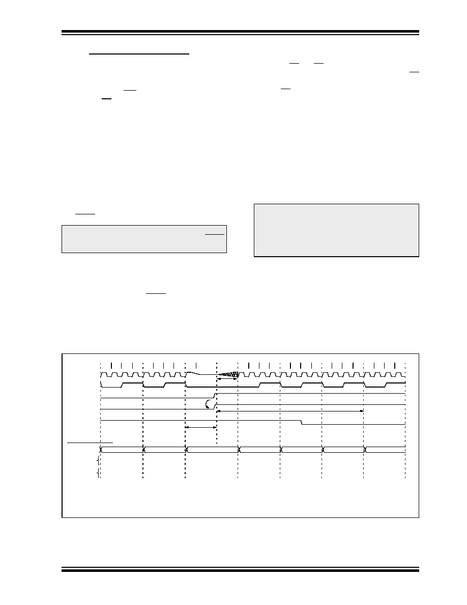
FIGURE 10-19: WAKE-UP FROM SLEEP THROUGH INTERRUPT
Q1
Q2
Q3 Q4
Q1 Q2
Q3
Q4
Q1
Q2 Q3 Q4
Q1 Q2 Q3 Q4
Q1
Q2 Q3
Q4
Q1 Q2
Q3
Q4
OSC1
CLKOUT(4)
INT pin
INTF flag
(INTCON<1>)
GIE bit
(INTCON<7>)
INSTRUCTION FLOW
PC
Instruction
fetched
Instruction
executed
PC
PC+1
PC+2
Inst(PC) = SLEEP
Inst(PC - 1)
Inst(PC + 1)
SLEEP
Processor in
SLEEP
Interrupt Latency
Inst(PC + 2)
Inst(PC + 1)
Inst(0004h)
Inst(0005h)
Inst(0004h)
Dummy cycle
PC + 2
0004h
0005h
Dummy cycle
TOST(2)
PC+2
Note 1:
XT, HS or LP oscillator mode assumed.
2:
TOST = 1024TOSC (drawing not to scale) This delay does not occur for RC osc mode.
3:
GIE = ’1’ assumed. In this case after wake- up, the processor jumps to the interrupt routine. If GIE = ’0’, execution will continue in-line.
4:
CLKOUT is not available in these osc modes, but shown here for timing reference.
相关PDF资料 |
PDF描述 |
|---|---|
| ADG508FBNZ | IC MULTIPLEXER 8X1 16DIP |
| VI-B2Z-IX-B1 | CONVERTER MOD DC/DC 2V 30W |
| PIC16F946T-I/PT | IC PIC MCU FLASH 8KX14 64TQFP |
| ADG1434YRUZ | IC SWITCH QUAD SPDT 20TSSOP |
| DSPIC33FJ12MC202T-I/SS | IC DSPIC MCU/DSP 12K 28SSOP |
相关代理商/技术参数 |
参数描述 |
|---|---|
| PIC16CE625T-20/SO | 功能描述:8位微控制器 -MCU 3.5KB 128 RAM 13 I/O RoHS:否 制造商:Silicon Labs 核心:8051 处理器系列:C8051F39x 数据总线宽度:8 bit 最大时钟频率:50 MHz 程序存储器大小:16 KB 数据 RAM 大小:1 KB 片上 ADC:Yes 工作电源电压:1.8 V to 3.6 V 工作温度范围:- 40 C to + 105 C 封装 / 箱体:QFN-20 安装风格:SMD/SMT |
| PIC16CE625T-20/SS | 功能描述:8位微控制器 -MCU 3.5KB 128 RAM 13 I/O RoHS:否 制造商:Silicon Labs 核心:8051 处理器系列:C8051F39x 数据总线宽度:8 bit 最大时钟频率:50 MHz 程序存储器大小:16 KB 数据 RAM 大小:1 KB 片上 ADC:Yes 工作电源电压:1.8 V to 3.6 V 工作温度范围:- 40 C to + 105 C 封装 / 箱体:QFN-20 安装风格:SMD/SMT |
| PIC16CE625T-20E/SO | 功能描述:8位微控制器 -MCU 3.5KB 128 RAM 13 I/O RoHS:否 制造商:Silicon Labs 核心:8051 处理器系列:C8051F39x 数据总线宽度:8 bit 最大时钟频率:50 MHz 程序存储器大小:16 KB 数据 RAM 大小:1 KB 片上 ADC:Yes 工作电源电压:1.8 V to 3.6 V 工作温度范围:- 40 C to + 105 C 封装 / 箱体:QFN-20 安装风格:SMD/SMT |
| PIC16CE625T-20E/SS | 功能描述:8位微控制器 -MCU 3.5KB 128 RAM 13 I/O RoHS:否 制造商:Silicon Labs 核心:8051 处理器系列:C8051F39x 数据总线宽度:8 bit 最大时钟频率:50 MHz 程序存储器大小:16 KB 数据 RAM 大小:1 KB 片上 ADC:Yes 工作电源电压:1.8 V to 3.6 V 工作温度范围:- 40 C to + 105 C 封装 / 箱体:QFN-20 安装风格:SMD/SMT |
| PIC16CE625T-20I/SO | 功能描述:8位微控制器 -MCU 3.5KB 128 RAM 13 I/O RoHS:否 制造商:Silicon Labs 核心:8051 处理器系列:C8051F39x 数据总线宽度:8 bit 最大时钟频率:50 MHz 程序存储器大小:16 KB 数据 RAM 大小:1 KB 片上 ADC:Yes 工作电源电压:1.8 V to 3.6 V 工作温度范围:- 40 C to + 105 C 封装 / 箱体:QFN-20 安装风格:SMD/SMT |
发布紧急采购,3分钟左右您将得到回复。