参数资料
| 型号: | PIC16CR77T-I/ML |
| 厂商: | Microchip Technology |
| 文件页数: | 17/172页 |
| 文件大小: | 0K |
| 描述: | IC PIC MCU 8KX14 44QFN |
| 标准包装: | 1,600 |
| 系列: | PIC® 16C |
| 核心处理器: | PIC |
| 芯体尺寸: | 8-位 |
| 速度: | 20MHz |
| 连通性: | I²C,SPI,UART/USART |
| 外围设备: | 欠压检测/复位,POR,PWM,WDT |
| 输入/输出数: | 33 |
| 程序存储器容量: | 14KB(8K x 14) |
| 程序存储器类型: | ROM |
| RAM 容量: | 368 x 8 |
| 电压 - 电源 (Vcc/Vdd): | 2 V ~ 5.5 V |
| 数据转换器: | A/D 8x8b |
| 振荡器型: | 内部 |
| 工作温度: | -40°C ~ 85°C |
| 封装/外壳: | 44-VQFN 裸露焊盘 |
| 包装: | 带卷 (TR) |
第1页第2页第3页第4页第5页第6页第7页第8页第9页第10页第11页第12页第13页第14页第15页第16页当前第17页第18页第19页第20页第21页第22页第23页第24页第25页第26页第27页第28页第29页第30页第31页第32页第33页第34页第35页第36页第37页第38页第39页第40页第41页第42页第43页第44页第45页第46页第47页第48页第49页第50页第51页第52页第53页第54页第55页第56页第57页第58页第59页第60页第61页第62页第63页第64页第65页第66页第67页第68页第69页第70页第71页第72页第73页第74页第75页第76页第77页第78页第79页第80页第81页第82页第83页第84页第85页第86页第87页第88页第89页第90页第91页第92页第93页第94页第95页第96页第97页第98页第99页第100页第101页第102页第103页第104页第105页第106页第107页第108页第109页第110页第111页第112页第113页第114页第115页第116页第117页第118页第119页第120页第121页第122页第123页第124页第125页第126页第127页第128页第129页第130页第131页第132页第133页第134页第135页第136页第137页第138页第139页第140页第141页第142页第143页第144页第145页第146页第147页第148页第149页第150页第151页第152页第153页第154页第155页第156页第157页第158页第159页第160页第161页第162页第163页第164页第165页第166页第167页第168页第169页第170页第171页第172页
2007 Microchip Technology Inc.
DS39599G-page 111
PIC18F2220/2320/4220/4320
10.5
PORTE, TRISE and LATE
Registers
PORTE is available only in PIC18F4X20 devices.
PIC18F2X20 devices always will read back 0x00 from
PORTE.
For PIC18F4X20 devices, PORTE is a 4-bit wide port.
Three pins (RE0/AN5/RD, RE1/AN6/WR and RE2/
AN7/CS) are individually configurable as inputs or out-
puts. These pins have Schmitt Trigger input buffers.
When selected as an analog input, these pins will read
as ‘0’s.
The corresponding Data Direction register is TRISE.
Setting a TRISE bit (= 1) will make the corresponding
PORTE pin an input (i.e., put the corresponding output
driver in a high-impedance mode). Clearing a TRISE bit
(= 0) will make the corresponding PORTE pin an output
(i.e., put the contents of the output latch on the selected
pin).
TRISE controls the direction of the RE pins even when
they are being used as analog inputs. The user must
make sure to keep the pins configured as inputs when
using them as analog inputs.
The upper four bits of the TRISE register also control
the operation of the Parallel Slave Port. Their operation
is explained in Register 10-1.
The Data Latch register (LATE) is also memory
mapped. Read-modify-write operations on the LATE
register read and write the latched output value for
PORTE.
The fourth pin of PORTE (MCLR/VPP/RE3) is an input
only pin. Its operation is controlled by the MCLRE Con-
figuration
bit
in
Configuration
Register
3H
(CONFIG3H<7>). When selected as a port pin
(MCLRE = 0), it functions as a digital input only pin; as
such, it does not have TRIS or LAT bits associated with
its operation. Otherwise, it functions as the device’s
Master Clear input. In either configuration, RE3 also
functions as the programming voltage input during
programming.
EXAMPLE 10-5:
INITIALIZING PORTE
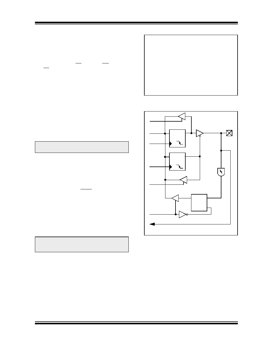
FIGURE 10-13:
BLOCK DIAGRAM OF
RE2:RE0 PINS
Note:
On a Power-on Reset, RE2:RE0 are
configured as analog inputs.
Note:
On a Power-on Reset, RE3 is enabled as
a digital input only if Master Clear
functionality is disabled.
CLRF
PORTE
; Initialize PORTE by
; clearing output
; data latches
CLRF
LATE
; Alternate method
; to clear output
; data latches
MOVLW
0x0A
; Configure A/D
MOVWF
ADCON1 ; for digital inputs
MOVLW
0x03
; Value used to
; initialize data
; direction
MOVWF
TRISC
; Set RE<0> as inputs
; RE<1> as outputs
; RE<2> as inputs
Data
Bus
WR LATE
WR TRISE
RD PORTE
Data Latch
TRIS Latch
RD TRISE
Schmitt
Trigger
Input
Buffer
Q
D
CK
Q
D
CK
EN
QD
EN
I/O pin(1)
RD LATE
or
PORTE
To Analog Converter
Note 1:
I/O pins have diode protection to VDD and VSS.
相关PDF资料 |
PDF描述 |
|---|---|
| PIC24F16KA102-I/SO | IC PIC MCU FLASH 16K 28-SOIC |
| PIC18F45K20-I/PT | IC PIC MCU FLASH 16KX16 44TQFP |
| PIC16CR77-I/PT | IC PIC MCU 8KX14 44TQFP |
| PIC16F884-I/ML | IC PIC MCU FLASH 4KX14 44QFN |
| PIC16CR77-I/P | IC PIC MCU 8KX14 40DIP |
相关代理商/技术参数 |
参数描述 |
|---|---|
| PIC16CR83T-04/SO023 | 制造商:Microchip Technology Inc 功能描述: |
| PIC16F | 制造商:Microchip Technology Inc 功能描述:Microchip PIC16F677-I/P Microcontroller |
| PIC16F1454-E/ML | 制造商:Microchip Technology Inc 功能描述:7 KB FLASH, 512 BYTES RAM, 48 MHZ INT. OSC, 12 I/0, ENHANCED - Rail/Tube 制造商:Microchip Technology Inc 功能描述:IC MCU 8BIT 7KB FLASH 16QFN |
| PIC16F1454-E/P | 制造商:Microchip Technology Inc 功能描述:7 KB FLASH, 512 BYTES RAM, 48 MHZ INT. OSC, 12 I/0, ENHANCED - Rail/Tube 制造商:Microchip Technology Inc 功能描述:IC MCU 8BIT 7KB FLASH 14PDIP |
| PIC16F1454-E/SL | 制造商:Microchip Technology Inc 功能描述:7 KB FLASH, 512 BYTES RAM, 48 MHZ INT. OSC, 12 I/0, ENHANCED - Rail/Tube 制造商:Microchip Technology Inc 功能描述:IC MCU 8BIT 7KB FLASH 14SOIC |
发布紧急采购,3分钟左右您将得到回复。