- 您现在的位置:买卖IC网 > PDF目录11617 > PIC16F1823T-I/SL (Microchip Technology)MCU 8BIT 8K FLASH 14SOIC PDF资料下载
参数资料
| 型号: | PIC16F1823T-I/SL |
| 厂商: | Microchip Technology |
| 文件页数: | 24/109页 |
| 文件大小: | 0K |
| 描述: | MCU 8BIT 8K FLASH 14SOIC |
| 标准包装: | 2,600 |
| 系列: | PIC® XLP™ 16F |
| 核心处理器: | PIC |
| 芯体尺寸: | 8-位 |
| 速度: | 32MHz |
| 连通性: | I²C,LIN,SPI,UART/USART |
| 外围设备: | 欠压检测/复位,POR,PWM,WDT |
| 输入/输出数: | 12 |
| 程序存储器容量: | 3.5KB(2K x 14) |
| 程序存储器类型: | 闪存 |
| EEPROM 大小: | 256 x 8 |
| RAM 容量: | 128 x 8 |
| 电压 - 电源 (Vcc/Vdd): | 1.8 V ~ 5.5 V |
| 数据转换器: | A/D 8x10b |
| 振荡器型: | 内部 |
| 工作温度: | -40°C ~ 85°C |
| 封装/外壳: | 14-SOIC(0.154",3.90mm 宽) |
| 包装: | 带卷 (TR) |
第1页第2页第3页第4页第5页第6页第7页第8页第9页第10页第11页第12页第13页第14页第15页第16页第17页第18页第19页第20页第21页第22页第23页当前第24页第25页第26页第27页第28页第29页第30页第31页第32页第33页第34页第35页第36页第37页第38页第39页第40页第41页第42页第43页第44页第45页第46页第47页第48页第49页第50页第51页第52页第53页第54页第55页第56页第57页第58页第59页第60页第61页第62页第63页第64页第65页第66页第67页第68页第69页第70页第71页第72页第73页第74页第75页第76页第77页第78页第79页第80页第81页第82页第83页第84页第85页第86页第87页第88页第89页第90页第91页第92页第93页第94页第95页第96页第97页第98页第99页第100页第101页第102页第103页第104页第105页第106页第107页第108页第109页
212
7674F–AVR–09/09
ATmega164P/324P/644P
The MSB of the address byte is transmitted first. Slave addresses can freely be allocated by the
designer, but the address 0000 000 is reserved for a general call.
When a general call is issued, all slaves should respond by pulling the SDA line low in the ACK
cycle. A general call is used when a Master wishes to transmit the same message to several
slaves in the system. When the general call address followed by a Write bit is transmitted on the
bus, all slaves set up to acknowledge the general call will pull the SDA line low in the ack cycle.
The following data packets will then be received by all the slaves that acknowledged the general
call. Note that transmitting the general call address followed by a Read bit is meaningless, as
this would cause contention if several slaves started transmitting different data.
All addresses of the format 1111 xxx should be reserved for future purposes.
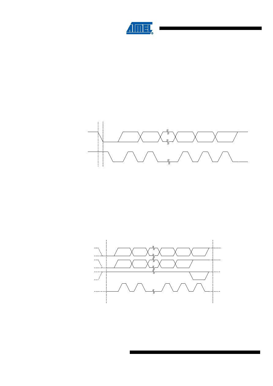
Figure 19-4. Address Packet Format
19.3.4
Data Packet Format
All data packets transmitted on the TWI bus are nine bits long, consisting of one data byte and
an acknowledge bit. During a data transfer, the Master generates the clock and the START and
STOP conditions, while the Receiver is responsible for acknowledging the reception. An
Acknowledge (ACK) is signalled by the Receiver pulling the SDA line low during the ninth SCL
cycle. If the Receiver leaves the SDA line high, a NACK is signalled. When the Receiver has
received the last byte, or for some reason cannot receive any more bytes, it should inform the
Transmitter by sending a NACK after the final byte. The MSB of the data byte is transmitted first.
Figure 19-5. Data Packet Format
SDA
SCL
START
12
7
8
9
Addr MSB
Addr LSB
R/W
ACK
12
78
9
Data MSB
Data LSB
ACK
Aggregate
SDA
SDA from
Transmitter
SDA from
Receiver
SCL from
Master
SLA+R/W
Data Byte
STOP, REPEATED
START or Next
Data Byte
相关PDF资料 |
PDF描述 |
|---|---|
| PIC16F616-E/ML | IC PIC MCU FLASH 2KX14 16QFN |
| PIC16F1507-E/ML | IC MCU 8BIT 3.5KB FLASH 20QFN |
| MS27484T24B4S | CONN PLUG 56POS STRAIGHT W/SCKT |
| MS27468T19B66S | CONN RCPT 66POS JAM NUT W/SCKT |
| MS27484T24F4S | CONN PLUG 56POS STRAIGHT W/SCKT |
相关代理商/技术参数 |
参数描述 |
|---|---|
| PIC16F1824-E/ML | 功能描述:8位微控制器 -MCU 7KB Flash 256b RAM 32 MHz Int. Osc RoHS:否 制造商:Silicon Labs 核心:8051 处理器系列:C8051F39x 数据总线宽度:8 bit 最大时钟频率:50 MHz 程序存储器大小:16 KB 数据 RAM 大小:1 KB 片上 ADC:Yes 工作电源电压:1.8 V to 3.6 V 工作温度范围:- 40 C to + 105 C 封装 / 箱体:QFN-20 安装风格:SMD/SMT |
| PIC16F1824-E/P | 功能描述:8位微控制器 -MCU 7KB Flash 256b RAM 32 MHz Int. Osc RoHS:否 制造商:Silicon Labs 核心:8051 处理器系列:C8051F39x 数据总线宽度:8 bit 最大时钟频率:50 MHz 程序存储器大小:16 KB 数据 RAM 大小:1 KB 片上 ADC:Yes 工作电源电压:1.8 V to 3.6 V 工作温度范围:- 40 C to + 105 C 封装 / 箱体:QFN-20 安装风格:SMD/SMT |
| PIC16F1824-E/SL | 功能描述:8位微控制器 -MCU 7KB Flash 256b RAM 32 MHz Int. Osc RoHS:否 制造商:Silicon Labs 核心:8051 处理器系列:C8051F39x 数据总线宽度:8 bit 最大时钟频率:50 MHz 程序存储器大小:16 KB 数据 RAM 大小:1 KB 片上 ADC:Yes 工作电源电压:1.8 V to 3.6 V 工作温度范围:- 40 C to + 105 C 封装 / 箱体:QFN-20 安装风格:SMD/SMT |
| PIC16F1824-E/ST | 功能描述:8位微控制器 -MCU 7KB Flash 256b RAM 32 MHz Int. Osc RoHS:否 制造商:Silicon Labs 核心:8051 处理器系列:C8051F39x 数据总线宽度:8 bit 最大时钟频率:50 MHz 程序存储器大小:16 KB 数据 RAM 大小:1 KB 片上 ADC:Yes 工作电源电压:1.8 V to 3.6 V 工作温度范围:- 40 C to + 105 C 封装 / 箱体:QFN-20 安装风格:SMD/SMT |
| PIC16F1824-I/ML | 功能描述:8位微控制器 -MCU 7 KB Flash 256b RAM 32 MHz Int. Osc RoHS:否 制造商:Silicon Labs 核心:8051 处理器系列:C8051F39x 数据总线宽度:8 bit 最大时钟频率:50 MHz 程序存储器大小:16 KB 数据 RAM 大小:1 KB 片上 ADC:Yes 工作电源电压:1.8 V to 3.6 V 工作温度范围:- 40 C to + 105 C 封装 / 箱体:QFN-20 安装风格:SMD/SMT |
发布紧急采购,3分钟左右您将得到回复。