- 您现在的位置:买卖IC网 > PDF目录11604 > PIC16F1825T-I/SL (Microchip Technology)MCU PIC 14K FLASH 1K RAM 14SOIC PDF资料下载
参数资料
| 型号: | PIC16F1825T-I/SL |
| 厂商: | Microchip Technology |
| 文件页数: | 36/208页 |
| 文件大小: | 0K |
| 描述: | MCU PIC 14K FLASH 1K RAM 14SOIC |
| 标准包装: | 2,600 |
| 系列: | PIC® XLP™ mTouch™ 16F |
| 核心处理器: | PIC |
| 芯体尺寸: | 8-位 |
| 速度: | 32MHz |
| 连通性: | I²C,LIN,SPI,UART/USART |
| 外围设备: | 欠压检测/复位,POR,PWM,WDT |
| 输入/输出数: | 11 |
| 程序存储器容量: | 14KB(8K x 14) |
| 程序存储器类型: | 闪存 |
| EEPROM 大小: | 256 x 8 |
| RAM 容量: | 1K x 8 |
| 电压 - 电源 (Vcc/Vdd): | 1.8 V ~ 5.5 V |
| 数据转换器: | A/D 8x10b |
| 振荡器型: | 内部 |
| 工作温度: | -40°C ~ 85°C |
| 封装/外壳: | 14-SOIC(0.154",3.90mm 宽) |
| 包装: | 带卷 (TR) |
第1页第2页第3页第4页第5页第6页第7页第8页第9页第10页第11页第12页第13页第14页第15页第16页第17页第18页第19页第20页第21页第22页第23页第24页第25页第26页第27页第28页第29页第30页第31页第32页第33页第34页第35页当前第36页第37页第38页第39页第40页第41页第42页第43页第44页第45页第46页第47页第48页第49页第50页第51页第52页第53页第54页第55页第56页第57页第58页第59页第60页第61页第62页第63页第64页第65页第66页第67页第68页第69页第70页第71页第72页第73页第74页第75页第76页第77页第78页第79页第80页第81页第82页第83页第84页第85页第86页第87页第88页第89页第90页第91页第92页第93页第94页第95页第96页第97页第98页第99页第100页第101页第102页第103页第104页第105页第106页第107页第108页第109页第110页第111页第112页第113页第114页第115页第116页第117页第118页第119页第120页第121页第122页第123页第124页第125页第126页第127页第128页第129页第130页第131页第132页第133页第134页第135页第136页第137页第138页第139页第140页第141页第142页第143页第144页第145页第146页第147页第148页第149页第150页第151页第152页第153页第154页第155页第156页第157页第158页第159页第160页第161页第162页第163页第164页第165页第166页第167页第168页第169页第170页第171页第172页第173页第174页第175页第176页第177页第178页第179页第180页第181页第182页第183页第184页第185页第186页第187页第188页第189页第190页第191页第192页第193页第194页第195页第196页第197页第198页第199页第200页第201页第202页第203页第204页第205页第206页第207页第208页
155
ATmega8515(L)
2512K–AVR–01/10
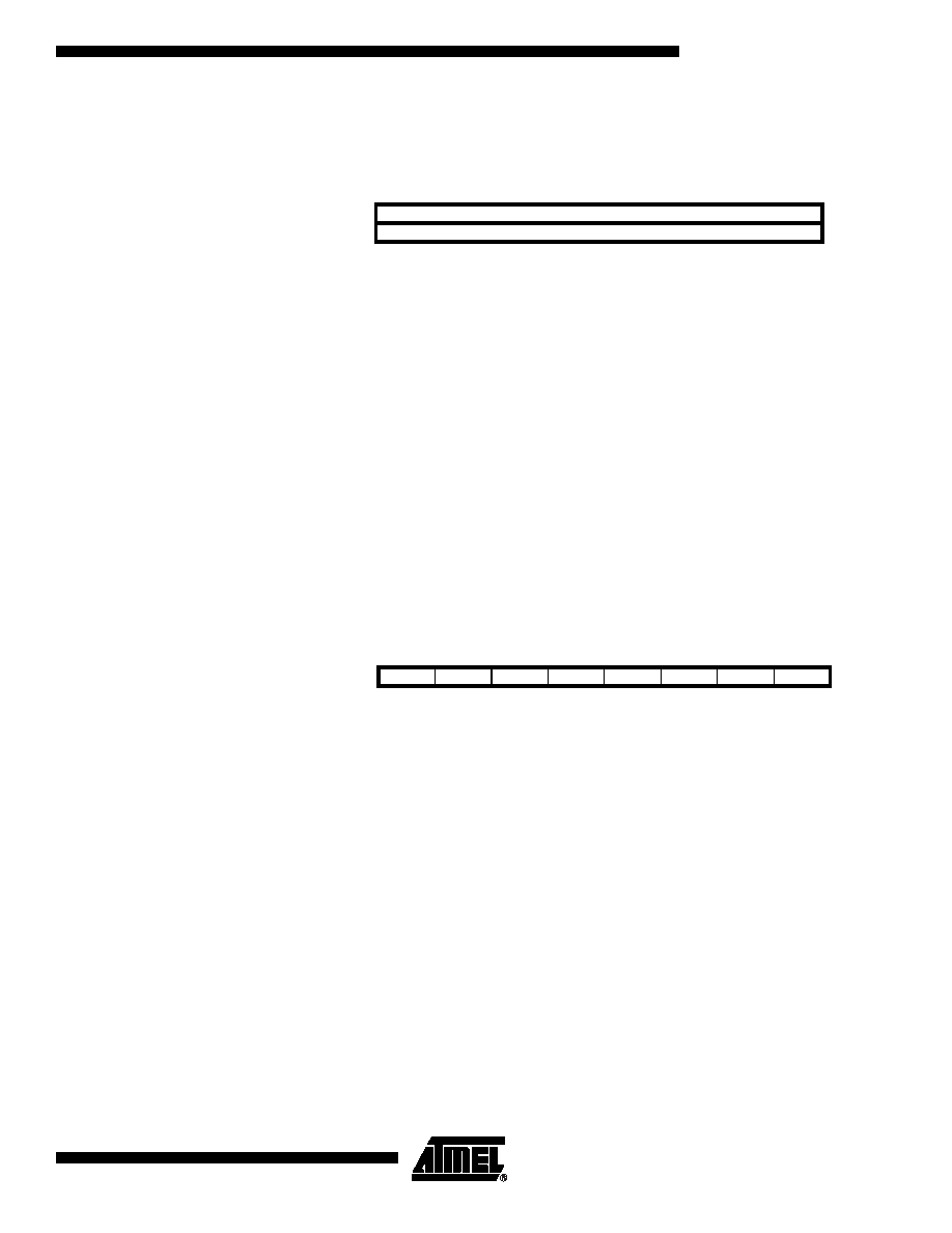
USART Register
Description
USART I/O Data Register –
UDR
The USART Transmit Data Buffer Register and USART Receive Data Buffer Registers
share the same I/O address referred to as USART Data Register or UDR. The Transmit
Data Buffer Register (TXB) will be the destination for data written to the UDR Register
location. Reading the UDR Register location will return the contents of the Receive Data
Buffer Register (RXB).
For 5-, 6-, or 7-bit characters the upper unused bits will be ignored by the Transmitter
and set to zero by the Receiver.
The transmit buffer can only be written when the UDRE Flag in the UCSRA Register is
set. Data written to UDR when the UDRE Flag is not set, will be ignored by the USART
Transmitter. When data is written to the transmit buffer, and the Transmitter is enabled,
the Transmitter will load the data into the Transmit Shift Register when the Shift Register
is empty. Then the data will be serially transmitted on the TxD pin.
The receive buffer consists of a two level FIFO. The FIFO will change its state whenever
the receive buffer is accessed. Due to this behavior of the receive buffer, do not use
read modify write instructions (SBI and CBI) on this location. Be careful when using bit
test instructions (SBIC and SBIS), since these also will change the state of the FIFO.
USART Control and Status
Register A – UCSRA
Bit 7 – RXC: USART Receive Complete
This flag bit is set when there are unread data in the receive buffer and cleared when the
receive buffer is empty (i.e., does not contain any unread data). If the Receiver is dis-
abled, the receive buffer will be flushed and consequently the RXC bit will become zero.
The RXC Flag can be used to generate a Receive Complete interrupt (see description of
the RXCIE bit).
Bit 6 – TXC: USART Transmit Complete
This flag bit is set when the entire frame in the Transmit Shift Register has been shifted
out and there are no new data currently present in the transmit buffer (UDR). The TXC
Flag bit is automatically cleared when a transmit complete interrupt is executed, or it can
be cleared by writing a one to its bit location. The TXC Flag can generate a Transmit
Complete interrupt (see description of the TXCIE bit).
Bit 5 – UDRE: USART Data Register Empty
The UDRE Flag indicates if the transmit buffer (UDR) is ready to receive new data. If
UDRE is one, the buffer is empty, and therefore ready to be written. The UDRE Flag can
generate a Data Register Empty interrupt (see description of the UDRIE bit).
UDRE is set after a reset to indicate that the Transmitter is ready.
Bit 4 – FE: Frame Error
Bit
7654
3210
RXB[7:0]
UDR (Read)
TXB[7:0]
UDR (Write)
Read/Write
R/W
Initial Value
0000
Bit
7654
321
0
RXC
TXC
UDRE
FE
DOR
PE
U2X
MPCM
UCSRA
Read/Write
R
R/W
R
R/W
Initial Value
0010
000
0
相关PDF资料 |
PDF描述 |
|---|---|
| PIC16F1824T-I/ST | IC MCU 8BIT 7KB FLASH 14TSSOP |
| D38999/24MG11SN | CONN RCPT 11POS JAM NUT W/SCKT |
| PIC16LF1824T-I/ST | IC MCU 8BIT 7KB FLASH 14TSSOP |
| MAX9174EUB+T | IC SPLITTER 1:2 LVDS 10-UMAX |
| ISL33002IRTZ-T | IC BUS BUFF HOTSWAP 2WR 8TDFN |
相关代理商/技术参数 |
参数描述 |
|---|---|
| PIC16F1826-E/ML | 功能描述:8位微控制器 -MCU 3.5KB Flash 256 byte 32 MHz Int. Osc RoHS:否 制造商:Silicon Labs 核心:8051 处理器系列:C8051F39x 数据总线宽度:8 bit 最大时钟频率:50 MHz 程序存储器大小:16 KB 数据 RAM 大小:1 KB 片上 ADC:Yes 工作电源电压:1.8 V to 3.6 V 工作温度范围:- 40 C to + 105 C 封装 / 箱体:QFN-20 安装风格:SMD/SMT |
| PIC16F1826-E/MQ | 功能描述:8位微控制器 -MCU 3.5KB Flash 256 byte 32 MHz Int. Osc RoHS:否 制造商:Silicon Labs 核心:8051 处理器系列:C8051F39x 数据总线宽度:8 bit 最大时钟频率:50 MHz 程序存储器大小:16 KB 数据 RAM 大小:1 KB 片上 ADC:Yes 工作电源电压:1.8 V to 3.6 V 工作温度范围:- 40 C to + 105 C 封装 / 箱体:QFN-20 安装风格:SMD/SMT |
| PIC16F1826-E/MV | 功能描述:8位微控制器 -MCU 3.5KB Flash 256 RAM RoHS:否 制造商:Silicon Labs 核心:8051 处理器系列:C8051F39x 数据总线宽度:8 bit 最大时钟频率:50 MHz 程序存储器大小:16 KB 数据 RAM 大小:1 KB 片上 ADC:Yes 工作电源电压:1.8 V to 3.6 V 工作温度范围:- 40 C to + 105 C 封装 / 箱体:QFN-20 安装风格:SMD/SMT |
| PIC16F1826-E/P | 功能描述:8位微控制器 -MCU 3.5KB Flash 256 byte 32 MHz Int. Osc RoHS:否 制造商:Silicon Labs 核心:8051 处理器系列:C8051F39x 数据总线宽度:8 bit 最大时钟频率:50 MHz 程序存储器大小:16 KB 数据 RAM 大小:1 KB 片上 ADC:Yes 工作电源电压:1.8 V to 3.6 V 工作温度范围:- 40 C to + 105 C 封装 / 箱体:QFN-20 安装风格:SMD/SMT |
| PIC16F1826-E/P | 制造商:Microchip Technology Inc 功能描述:8-BIT MICROCONTROLLER |
发布紧急采购,3分钟左右您将得到回复。