- 您现在的位置:买卖IC网 > PDF目录11620 > PIC16F526T-I/MG (Microchip Technology)MCU PIC 1.5K FLASH 3X3 16QFN PDF资料下载
参数资料
| 型号: | PIC16F526T-I/MG |
| 厂商: | Microchip Technology |
| 文件页数: | 29/122页 |
| 文件大小: | 0K |
| 描述: | MCU PIC 1.5K FLASH 3X3 16QFN |
| 标准包装: | 3,300 |
| 系列: | PIC® 16F |
| 核心处理器: | PIC |
| 芯体尺寸: | 8-位 |
| 速度: | 20MHz |
| 外围设备: | POR,WDT |
| 输入/输出数: | 11 |
| 程序存储器容量: | 1.5KB(1K x 12) |
| 程序存储器类型: | 闪存 |
| RAM 容量: | 67 x 8 |
| 电压 - 电源 (Vcc/Vdd): | 2 V ~ 5.5 V |
| 数据转换器: | A/D 3x8b |
| 振荡器型: | 内部 |
| 工作温度: | -40°C ~ 85°C |
| 封装/外壳: | 16-VFQFN 裸露焊盘 |
| 包装: | 带卷 (TR) |
第1页第2页第3页第4页第5页第6页第7页第8页第9页第10页第11页第12页第13页第14页第15页第16页第17页第18页第19页第20页第21页第22页第23页第24页第25页第26页第27页第28页当前第29页第30页第31页第32页第33页第34页第35页第36页第37页第38页第39页第40页第41页第42页第43页第44页第45页第46页第47页第48页第49页第50页第51页第52页第53页第54页第55页第56页第57页第58页第59页第60页第61页第62页第63页第64页第65页第66页第67页第68页第69页第70页第71页第72页第73页第74页第75页第76页第77页第78页第79页第80页第81页第82页第83页第84页第85页第86页第87页第88页第89页第90页第91页第92页第93页第94页第95页第96页第97页第98页第99页第100页第101页第102页第103页第104页第105页第106页第107页第108页第109页第110页第111页第112页第113页第114页第115页第116页第117页第118页第119页第120页第121页第122页
PIC16F526
DS41326E-page 14
2010 Microchip Technology Inc.
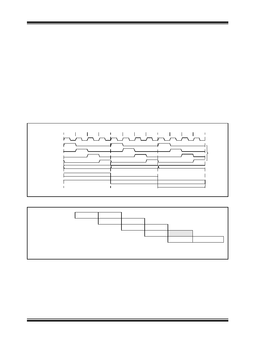
3.1
Clocking Scheme/Instruction
Cycle
The clock input (OSC1/CLKIN pin) is internally divided
by four to generate four non-overlapping quadrature
clocks, namely Q1, Q2, Q3 and Q4. Internally, the PC
is incremented every Q1 and the instruction is fetched
from program memory and latched into the instruction
register in Q4. It is decoded and executed during the
following Q1 through Q4. The clocks and instruction
execution flow is shown in Figure 3-2 and Example 3-1.
3.2
Instruction Flow/Pipelining
An instruction cycle consists of four Q cycles (Q1, Q2,
Q3 and Q4). The instruction fetch and execute are
pipelined such that fetch takes one instruction cycle,
while decode and execute take another instruction
cycle. However, due to the pipelining, each instruction
effectively executes in one cycle. If an instruction
causes the PC to change (e.g., GOTO), then two cycles
are required to complete the instruction (Example 3-1).
A fetch cycle begins with the PC incrementing in Q1.
In the execution cycle, the fetched instruction is latched
into the Instruction Register (IR) in cycle Q1. This
instruction is then decoded and executed during the
Q2, Q3 and Q4 cycles. Data memory is read during Q2
(operand read) and written during Q4 (destination
write).
FIGURE 3-2:
CLOCK/INSTRUCTION CYCLE
EXAMPLE 3-1:
INSTRUCTION PIPELINE FLOW
Q1
Q2
Q3
Q4
Q1
Q2
Q3
Q4
Q1
Q2
Q3
Q4
OSC1
Q1
Q2
Q3
Q4
PC
PC + 1
PC + 2
Fetch INST (PC)
Execute INST (PC – 1)
Fetch INST (PC + 1)
Execute INST (PC)
Fetch INST (PC + 2)
Execute INST (PC + 1)
Internal
Phase
Clock
All instructions are single cycle, except for any program branches. These take two cycles, since the fetch instruction
is “flushed” from the pipeline, while the new instruction is being fetched and then executed.
1. MOVLW 03H
Fetch 1
Execute 1
2. MOVWF PORTB
Fetch 2
Execute 2
3. CALL SUB_1
Fetch 3
Execute 3
4. BSF PORTB, BIT1
Fetch 4
Flush
Fetch SUB_1 Execute SUB_1
相关PDF资料 |
PDF描述 |
|---|---|
| PIC16HV610T-I/ST | IC PIC MCU FLASH 1KX14 14TSSOP |
| VI-J6F-IZ-B1 | CONVERTER MOD DC/DC 72V 25W |
| VI-J6F-IY-F3 | CONVERTER MOD DC/DC 72V 50W |
| PIC16F616-E/SL | IC PIC MCU FLASH 2KX14 14SOIC |
| PCA9509AGM,125 | IC I2C BUS/SMBUS REPEATER 8-XQFN |
相关代理商/技术参数 |
参数描述 |
|---|---|
| PIC16F527-E/ML | 制造商:Microchip Technology Inc 功能描述:IC MCU 8BIT 1.5KB FLASH 20QFN |
| PIC16F527-E/P | 制造商:Microchip Technology 功能描述:MCU 8-bit PIC16 PIC RISC 1.5KB Flash 2.5V/3.3V/5V 20-Pin PDIP Tube 制造商:Microchip Technology Inc 功能描述:1.5KB FLASH PROGRAM, 64B FLASH DATA, 8MHZ INTERNAL OSCILLATO - Rail/Tube 制造商:Microchip Technology Inc 功能描述:IC MCU 8BIT 1.5KB FLASH 20PDIP 制造商:Microchip Technology Inc 功能描述:8-bit Microcontrollers - MCU 8MHz Oscillator, 8b ADC 2x Comp, 2x Amps |
| PIC16F527-E/SO | 制造商:Microchip Technology Inc 功能描述:1.5KB FLASH PROGRAM, 64B FLASH DATA, 8MHZ INTERNAL OSCILLATO - Rail/Tube 制造商:Microchip Technology Inc 功能描述:IC MCU 8BIT 1.5KB FLASH 20SOIC |
| PIC16F527-I/ML | 功能描述:8位微控制器 -MCU 8MHz Oscillator, 8b ADC 2x Comp, 2x Amps RoHS:否 制造商:Silicon Labs 核心:8051 处理器系列:C8051F39x 数据总线宽度:8 bit 最大时钟频率:50 MHz 程序存储器大小:16 KB 数据 RAM 大小:1 KB 片上 ADC:Yes 工作电源电压:1.8 V to 3.6 V 工作温度范围:- 40 C to + 105 C 封装 / 箱体:QFN-20 安装风格:SMD/SMT |
| PIC16F527-I/P | 功能描述:8位微控制器 -MCU 8MHz Oscillator, 8b ADC 2x Comp, 2x Amps RoHS:否 制造商:Silicon Labs 核心:8051 处理器系列:C8051F39x 数据总线宽度:8 bit 最大时钟频率:50 MHz 程序存储器大小:16 KB 数据 RAM 大小:1 KB 片上 ADC:Yes 工作电源电压:1.8 V to 3.6 V 工作温度范围:- 40 C to + 105 C 封装 / 箱体:QFN-20 安装风格:SMD/SMT |
发布紧急采购,3分钟左右您将得到回复。