- 您现在的位置:买卖IC网 > PDF目录11510 > PIC16F72-E/SS (Microchip Technology)IC PIC MCU FLASH 2KX14 8-SSOP PDF资料下载
参数资料
| 型号: | PIC16F72-E/SS |
| 厂商: | Microchip Technology |
| 文件页数: | 123/136页 |
| 文件大小: | 0K |
| 描述: | IC PIC MCU FLASH 2KX14 8-SSOP |
| 产品培训模块: | Asynchronous Stimulus |
| 标准包装: | 47 |
| 系列: | PIC® 16F |
| 核心处理器: | PIC |
| 芯体尺寸: | 8-位 |
| 速度: | 20MHz |
| 连通性: | I²C,SPI |
| 外围设备: | 欠压检测/复位,POR,PWM,WDT |
| 输入/输出数: | 22 |
| 程序存储器容量: | 3.5KB(2K x 14) |
| 程序存储器类型: | 闪存 |
| RAM 容量: | 128 x 8 |
| 电压 - 电源 (Vcc/Vdd): | 4 V ~ 5.5 V |
| 数据转换器: | A/D 5x8b |
| 振荡器型: | 外部 |
| 工作温度: | -40°C ~ 125°C |
| 封装/外壳: | 28-SSOP(0.209",5.30mm 宽) |
| 包装: | 管件 |
第1页第2页第3页第4页第5页第6页第7页第8页第9页第10页第11页第12页第13页第14页第15页第16页第17页第18页第19页第20页第21页第22页第23页第24页第25页第26页第27页第28页第29页第30页第31页第32页第33页第34页第35页第36页第37页第38页第39页第40页第41页第42页第43页第44页第45页第46页第47页第48页第49页第50页第51页第52页第53页第54页第55页第56页第57页第58页第59页第60页第61页第62页第63页第64页第65页第66页第67页第68页第69页第70页第71页第72页第73页第74页第75页第76页第77页第78页第79页第80页第81页第82页第83页第84页第85页第86页第87页第88页第89页第90页第91页第92页第93页第94页第95页第96页第97页第98页第99页第100页第101页第102页第103页第104页第105页第106页第107页第108页第109页第110页第111页第112页第113页第114页第115页第116页第117页第118页第119页第120页第121页第122页当前第123页第124页第125页第126页第127页第128页第129页第130页第131页第132页第133页第134页第135页第136页
87
2535J–AVR–08/10
ATtiny13
14.6.2
ADC Voltage Reference
The reference voltage for the ADC (VREF) indicates the conversion range for the ADC. Single
ended channels that exceed VREF will result in codes close to 0x3FF. VREF can be selected as
either VCC, or internal 1.1V reference. The first ADC conversion result after switching reference
voltage source may be inaccurate, and the user is advised to discard this result.
14.7 ADC Noise Canceler
The ADC features a noise canceler that enables conversion during sleep mode to reduce noise
induced from the CPU core and other I/O peripherals. The noise canceler can be used with ADC
Noise Reduction and Idle mode. To make use of this feature, the following procedure should be
used:
Make sure that the ADC is enabled and is not busy converting. Single Conversion mode must
be selected and the ADC conversion complete interrupt must be enabled.
Enter ADC Noise Reduction mode (or Idle mode). The ADC will start a conversion once the
CPU has been halted.
If no other interrupts occur before the ADC conversion completes, the ADC interrupt will
wake up the CPU and execute the ADC Conversion Complete interrupt routine. If another
interrupt wakes up the CPU before the ADC conversion is complete, the interrupt will be
executed, and an ADC Conversion Complete interrupt request will be generated when the
ADC conversion completes. The CPU will remain in active mode until a new sleep command
is executed.
Note that the ADC will not be automatically turned off when entering other sleep modes than Idle
mode and ADC Noise Reduction mode. The user is advised to write zero to ADEN before enter-
ing such sleep modes to avoid excessive power consumption.
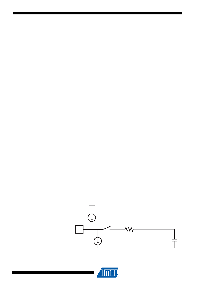
14.8 Analog Input Circuitry
The analog input circuitry for single ended channels is shown in Figure 14-8 An analog source
applied to ADCn is subjected to pin capacitance and input leakage of that pin, regardless if the
channel is chosen as input for the ADC, or not. When the channel is selected, the source drives
the S/H capacitor through the series resistance (combined resistance in input path).
Figure 14-8. Analog Input Circuitry
Note:
The capacitor in the figure depicts the total capacitance, including the sample/hold capacitor and
any stray or parasitic capacitance inside the device. The value given is worst case.
n
IIH
1..100 k
ohm
CS/H= 14 pF
IIL
相关PDF资料 |
PDF描述 |
|---|---|
| VI-J6M-IX-S | CONVERTER MOD DC/DC 10V 75W |
| VI-J6L-IX-S | CONVERTER MOD DC/DC 28V 75W |
| VI-J61-IX-S | CONVERTER MOD DC/DC 12V 75W |
| DG409DQ-T1-E3 | IC MULTIPLEXER DUAL 4X2 16TSSOP |
| VI-JWF-IX-S | CONVERTER MOD DC/DC 72V 75W |
相关代理商/技术参数 |
参数描述 |
|---|---|
| PIC16F72-I/ML | 功能描述:8位微控制器 -MCU 3.5KB 128 RAM 22 I/O RoHS:否 制造商:Silicon Labs 核心:8051 处理器系列:C8051F39x 数据总线宽度:8 bit 最大时钟频率:50 MHz 程序存储器大小:16 KB 数据 RAM 大小:1 KB 片上 ADC:Yes 工作电源电压:1.8 V to 3.6 V 工作温度范围:- 40 C to + 105 C 封装 / 箱体:QFN-20 安装风格:SMD/SMT |
| PIC16F72-I/MLG | 功能描述:8位微控制器 -MCU 3.5KB 128 RAM 22 I/O Lead Free Package RoHS:否 制造商:Silicon Labs 核心:8051 处理器系列:C8051F39x 数据总线宽度:8 bit 最大时钟频率:50 MHz 程序存储器大小:16 KB 数据 RAM 大小:1 KB 片上 ADC:Yes 工作电源电压:1.8 V to 3.6 V 工作温度范围:- 40 C to + 105 C 封装 / 箱体:QFN-20 安装风格:SMD/SMT |
| PIC16F72-I/SO | 功能描述:8位微控制器 -MCU 3.5KB 128 RAM 22 I/O RoHS:否 制造商:Silicon Labs 核心:8051 处理器系列:C8051F39x 数据总线宽度:8 bit 最大时钟频率:50 MHz 程序存储器大小:16 KB 数据 RAM 大小:1 KB 片上 ADC:Yes 工作电源电压:1.8 V to 3.6 V 工作温度范围:- 40 C to + 105 C 封装 / 箱体:QFN-20 安装风格:SMD/SMT |
| PIC16F72-I/SO | 制造商:Microchip Technology Inc 功能描述:8BIT FLASH MCU SMD 16F72 SOIC28 |
| PIC16F72-I/SOG | 功能描述:8位微控制器 -MCU 3.5KB 128 RAM 22 I/O Lead Free Package RoHS:否 制造商:Silicon Labs 核心:8051 处理器系列:C8051F39x 数据总线宽度:8 bit 最大时钟频率:50 MHz 程序存储器大小:16 KB 数据 RAM 大小:1 KB 片上 ADC:Yes 工作电源电压:1.8 V to 3.6 V 工作温度范围:- 40 C to + 105 C 封装 / 箱体:QFN-20 安装风格:SMD/SMT |
发布紧急采购,3分钟左右您将得到回复。