- 您现在的位置:买卖IC网 > PDF目录11510 > PIC16F72-E/SS (Microchip Technology)IC PIC MCU FLASH 2KX14 8-SSOP PDF资料下载
参数资料
| 型号: | PIC16F72-E/SS |
| 厂商: | Microchip Technology |
| 文件页数: | 129/136页 |
| 文件大小: | 0K |
| 描述: | IC PIC MCU FLASH 2KX14 8-SSOP |
| 产品培训模块: | Asynchronous Stimulus |
| 标准包装: | 47 |
| 系列: | PIC® 16F |
| 核心处理器: | PIC |
| 芯体尺寸: | 8-位 |
| 速度: | 20MHz |
| 连通性: | I²C,SPI |
| 外围设备: | 欠压检测/复位,POR,PWM,WDT |
| 输入/输出数: | 22 |
| 程序存储器容量: | 3.5KB(2K x 14) |
| 程序存储器类型: | 闪存 |
| RAM 容量: | 128 x 8 |
| 电压 - 电源 (Vcc/Vdd): | 4 V ~ 5.5 V |
| 数据转换器: | A/D 5x8b |
| 振荡器型: | 外部 |
| 工作温度: | -40°C ~ 125°C |
| 封装/外壳: | 28-SSOP(0.209",5.30mm 宽) |
| 包装: | 管件 |
第1页第2页第3页第4页第5页第6页第7页第8页第9页第10页第11页第12页第13页第14页第15页第16页第17页第18页第19页第20页第21页第22页第23页第24页第25页第26页第27页第28页第29页第30页第31页第32页第33页第34页第35页第36页第37页第38页第39页第40页第41页第42页第43页第44页第45页第46页第47页第48页第49页第50页第51页第52页第53页第54页第55页第56页第57页第58页第59页第60页第61页第62页第63页第64页第65页第66页第67页第68页第69页第70页第71页第72页第73页第74页第75页第76页第77页第78页第79页第80页第81页第82页第83页第84页第85页第86页第87页第88页第89页第90页第91页第92页第93页第94页第95页第96页第97页第98页第99页第100页第101页第102页第103页第104页第105页第106页第107页第108页第109页第110页第111页第112页第113页第114页第115页第116页第117页第118页第119页第120页第121页第122页第123页第124页第125页第126页第127页第128页当前第129页第130页第131页第132页第133页第134页第135页第136页
92
2535J–AVR–08/10
ATtiny13
Bits 4:2 – Res: Reserved Bits
These bits are reserved bits in the ATtiny13 and will always read as zero.
Bits 1:0 – MUX1:0: Analog Channel Selection Bits
The value of these bits selects which combination of analog inputs are connected to the ADC.
See Table 14-3 on page 92 for details. If these bits are changed during a conversion, the change
will not go in effect until this conversion is complete (ADIF in ADCSRA is set).
14.12.2
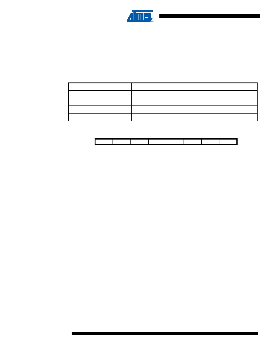
ADCSRA – ADC Control and Status Register A
Bit 7 – ADEN: ADC Enable
Writing this bit to one enables the ADC. By writing it to zero, the ADC is turned off. Turning the
ADC off while a conversion is in progress, will terminate this conversion.
Bit 6 – ADSC: ADC Start Conversion
In Single Conversion mode, write this bit to one to start each conversion. In Free Running mode,
write this bit to one to start the first conversion. The first conversion after ADSC has been written
after the ADC has been enabled, or if ADSC is written at the same time as the ADC is enabled,
will take 25 ADC clock cycles instead of the normal 13. This first conversion performs initializa-
tion of the ADC.
ADSC will read as one as long as a conversion is in progress. When the conversion is complete,
it returns to zero. Writing zero to this bit has no effect.
Bit 5 – ADATE: ADC Auto Trigger Enable
When this bit is written to one, Auto Triggering of the ADC is enabled. The ADC will start a con-
version on a positive edge of the selected trigger signal. The trigger source is selected by setting
the ADC Trigger Select bits, ADTS in ADCSRB.
Bit 4 – ADIF: ADC Interrupt Flag
This bit is set when an ADC conversion completes and the data registers are updated. The ADC
Conversion Complete Interrupt is executed if the ADIE bit and the I-bit in SREG are set. ADIF is
cleared by hardware when executing the corresponding interrupt handling vector. Alternatively,
ADIF is cleared by writing a logical one to the flag. Beware that if doing a Read-Modify-Write on
ADCSRA, a pending interrupt can be disabled. This also applies if the SBI and CBI instructions
are used.
Table 14-3.
Input Channel Selections
MUX1..0
Single Ended Input
00
ADC0 (PB5)
01
ADC1 (PB2)
10
ADC2 (PB4)
11
ADC3 (PB3)
Bit
76543210
ADEN
ADSC
ADATE
ADIF
ADIE
ADPS2
ADPS1
ADPS0
ADCSRA
Read/Write
R/W
Initial Value
00000000
相关PDF资料 |
PDF描述 |
|---|---|
| VI-J6M-IX-S | CONVERTER MOD DC/DC 10V 75W |
| VI-J6L-IX-S | CONVERTER MOD DC/DC 28V 75W |
| VI-J61-IX-S | CONVERTER MOD DC/DC 12V 75W |
| DG409DQ-T1-E3 | IC MULTIPLEXER DUAL 4X2 16TSSOP |
| VI-JWF-IX-S | CONVERTER MOD DC/DC 72V 75W |
相关代理商/技术参数 |
参数描述 |
|---|---|
| PIC16F72-I/ML | 功能描述:8位微控制器 -MCU 3.5KB 128 RAM 22 I/O RoHS:否 制造商:Silicon Labs 核心:8051 处理器系列:C8051F39x 数据总线宽度:8 bit 最大时钟频率:50 MHz 程序存储器大小:16 KB 数据 RAM 大小:1 KB 片上 ADC:Yes 工作电源电压:1.8 V to 3.6 V 工作温度范围:- 40 C to + 105 C 封装 / 箱体:QFN-20 安装风格:SMD/SMT |
| PIC16F72-I/MLG | 功能描述:8位微控制器 -MCU 3.5KB 128 RAM 22 I/O Lead Free Package RoHS:否 制造商:Silicon Labs 核心:8051 处理器系列:C8051F39x 数据总线宽度:8 bit 最大时钟频率:50 MHz 程序存储器大小:16 KB 数据 RAM 大小:1 KB 片上 ADC:Yes 工作电源电压:1.8 V to 3.6 V 工作温度范围:- 40 C to + 105 C 封装 / 箱体:QFN-20 安装风格:SMD/SMT |
| PIC16F72-I/SO | 功能描述:8位微控制器 -MCU 3.5KB 128 RAM 22 I/O RoHS:否 制造商:Silicon Labs 核心:8051 处理器系列:C8051F39x 数据总线宽度:8 bit 最大时钟频率:50 MHz 程序存储器大小:16 KB 数据 RAM 大小:1 KB 片上 ADC:Yes 工作电源电压:1.8 V to 3.6 V 工作温度范围:- 40 C to + 105 C 封装 / 箱体:QFN-20 安装风格:SMD/SMT |
| PIC16F72-I/SO | 制造商:Microchip Technology Inc 功能描述:8BIT FLASH MCU SMD 16F72 SOIC28 |
| PIC16F72-I/SOG | 功能描述:8位微控制器 -MCU 3.5KB 128 RAM 22 I/O Lead Free Package RoHS:否 制造商:Silicon Labs 核心:8051 处理器系列:C8051F39x 数据总线宽度:8 bit 最大时钟频率:50 MHz 程序存储器大小:16 KB 数据 RAM 大小:1 KB 片上 ADC:Yes 工作电源电压:1.8 V to 3.6 V 工作温度范围:- 40 C to + 105 C 封装 / 箱体:QFN-20 安装风格:SMD/SMT |
发布紧急采购,3分钟左右您将得到回复。