参数资料
| 型号: | PIC16F747-I/P |
| 厂商: | Microchip Technology |
| 文件页数: | 135/231页 |
| 文件大小: | 0K |
| 描述: | IC PIC MCU FLASH 4KX14 40DIP |
| 产品培训模块: | Asynchronous Stimulus 8-bit PIC® Microcontroller Portfolio |
| 标准包装: | 10 |
| 系列: | PIC® 16F |
| 核心处理器: | PIC |
| 芯体尺寸: | 8-位 |
| 速度: | 20MHz |
| 连通性: | I²C,SPI,UART/USART |
| 外围设备: | 欠压检测/复位,POR,PWM,WDT |
| 输入/输出数: | 36 |
| 程序存储器容量: | 7KB(4K x 14) |
| 程序存储器类型: | 闪存 |
| RAM 容量: | 368 x 8 |
| 电压 - 电源 (Vcc/Vdd): | 4 V ~ 5.5 V |
| 数据转换器: | A/D 14x10b |
| 振荡器型: | 内部 |
| 工作温度: | -40°C ~ 85°C |
| 封装/外壳: | 40-DIP(0.600",15.24mm) |
| 包装: | 管件 |
| 产品目录页面: | 640 (CN2011-ZH PDF) |
| 配用: | I3DBF777-ND - BOARD DAUGHTER ICEPIC3 DVA18XP400-ND - DEVICE ADAPTER 18F4220 PDIP 40LD 444-1001-ND - DEMO BOARD FOR PICMICRO MCU |
第1页第2页第3页第4页第5页第6页第7页第8页第9页第10页第11页第12页第13页第14页第15页第16页第17页第18页第19页第20页第21页第22页第23页第24页第25页第26页第27页第28页第29页第30页第31页第32页第33页第34页第35页第36页第37页第38页第39页第40页第41页第42页第43页第44页第45页第46页第47页第48页第49页第50页第51页第52页第53页第54页第55页第56页第57页第58页第59页第60页第61页第62页第63页第64页第65页第66页第67页第68页第69页第70页第71页第72页第73页第74页第75页第76页第77页第78页第79页第80页第81页第82页第83页第84页第85页第86页第87页第88页第89页第90页第91页第92页第93页第94页第95页第96页第97页第98页第99页第100页第101页第102页第103页第104页第105页第106页第107页第108页第109页第110页第111页第112页第113页第114页第115页第116页第117页第118页第119页第120页第121页第122页第123页第124页第125页第126页第127页第128页第129页第130页第131页第132页第133页第134页当前第135页第136页第137页第138页第139页第140页第141页第142页第143页第144页第145页第146页第147页第148页第149页第150页第151页第152页第153页第154页第155页第156页第157页第158页第159页第160页第161页第162页第163页第164页第165页第166页第167页第168页第169页第170页第171页第172页第173页第174页第175页第176页第177页第178页第179页第180页第181页第182页第183页第184页第185页第186页第187页第188页第189页第190页第191页第192页第193页第194页第195页第196页第197页第198页第199页第200页第201页第202页第203页第204页第205页第206页第207页第208页第209页第210页第211页第212页第213页第214页第215页第216页第217页第218页第219页第220页第221页第222页第223页第224页第225页第226页第227页第228页第229页第230页第231页
2009 Microchip Technology Inc.
DS39636D-page 225
PIC18F2X1X/4X1X
19.2
Comparator Operation
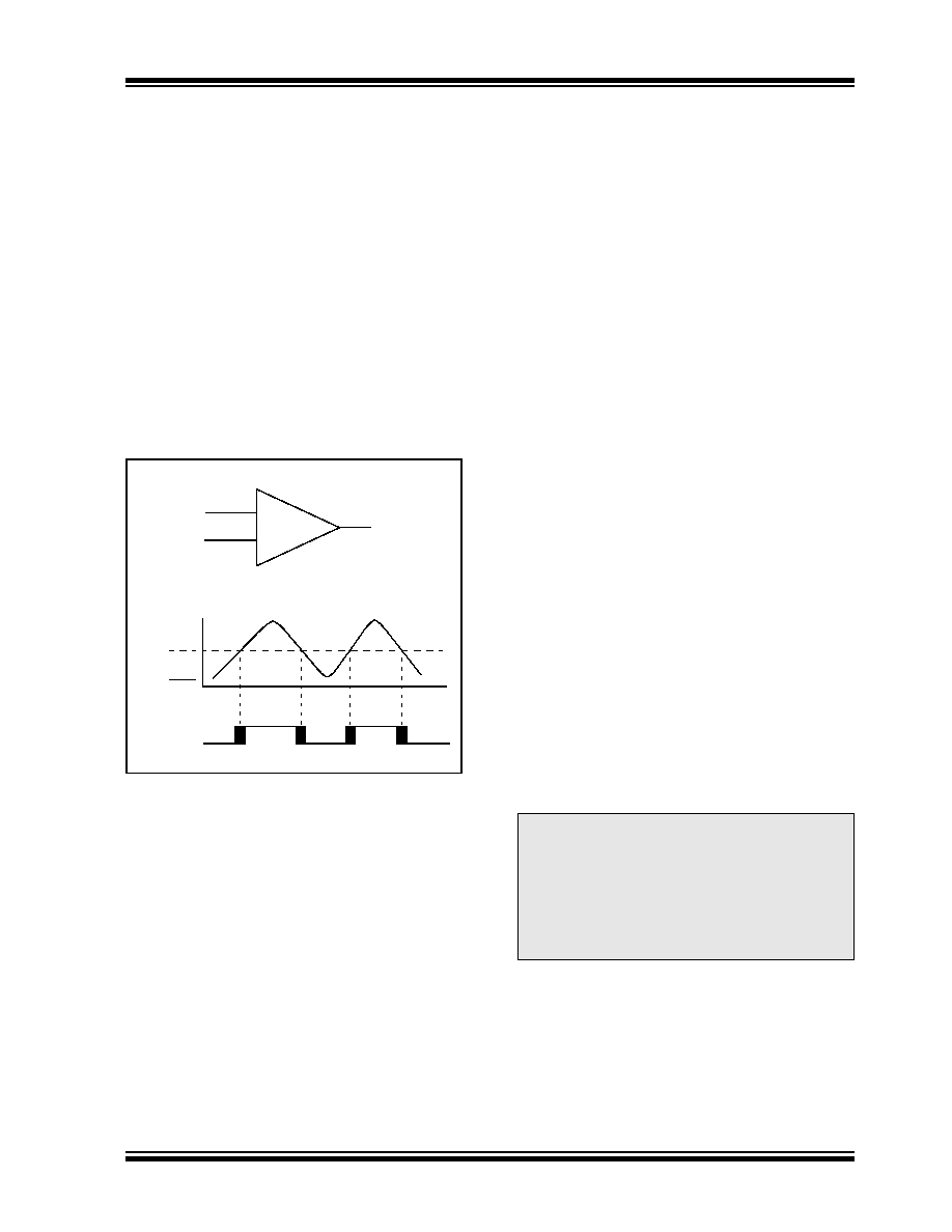
A single comparator is shown in Figure 19-2, along with
the relationship between the analog input levels and
the digital output. When the analog input at VIN+ is less
than the analog input VIN-, the output of the comparator
is a digital low level. When the analog input at VIN+ is
greater than the analog input VIN-, the output of the
comparator is a digital high level. The shaded areas of
the output of the comparator in Figure 19-2 represent
the uncertainty, due to input offsets and response time.
19.3
Comparator Reference
Depending on the comparator operating mode, either
an external or internal voltage reference may be used.
The analog signal present at VIN- is compared to the
signal at VIN+ and the digital output of the comparator
is adjusted accordingly (Figure 19-2).
FIGURE 19-2:
SINGLE COMPARATOR
19.3.1
EXTERNAL REFERENCE SIGNAL
When external voltage references are used, the
comparator module can be configured to have the com-
parators operate from the same or different reference
sources. However, threshold detector applications may
require the same reference. The reference signal must
be between VSS and VDD and can be applied to either
pin of the comparator(s).
19.3.2
INTERNAL REFERENCE SIGNAL
The comparator module also allows the selection of an
internally generated voltage reference from the
comparator voltage reference module. This module is
described in more detail in Section 20.0 “Comparator
The internal reference is only available in the mode
where four inputs are multiplexed to two comparators
(CM2:CM0 = 110). In this mode, the internal voltage
reference is applied to the VIN+ pin of both
comparators.
19.4
Comparator Response Time
Response time is the minimum time, after selecting a
new reference voltage or input source, before the
comparator output has a valid level. If the internal
reference is changed, the maximum delay of the
internal voltage reference must be considered when
using the comparator outputs. Otherwise, the
maximum delay of the comparators should be used
19.5
Comparator Outputs
The comparator outputs are read through the CMCON
register. These bits are read-only. The comparator
outputs may also be directly output to the RA4 and RA5
I/O pins. When enabled, multiplexors in the output path
of the RA4 and RA5 pins will switch and the output of
each pin will be the unsynchronized output of the
comparator.
The
uncertainty
of
each
of
the
comparators is related to the input offset voltage and
the response time given in the specifications.
Figure 19-3 shows the comparator output block
diagram.
The TRISA bits will still function as an output enable/
disable for the RA4 and RA5 pins while in this mode.
The polarity of the comparator outputs can be changed
using the C2INV and C1INV bits (CMCON<4:5>).
–
+
VIN
+
VIN
-
Output
VIN-
VIN+
Note 1: When reading the Port register, all pins
configured as analog inputs will read as a
‘0’. Pins configured as digital inputs will
convert an analog input according to the
Schmitt Trigger input specification.
2: Analog levels on any pin defined as a
digital input may cause the input buffer to
consume more current than is specified.
相关PDF资料 |
PDF描述 |
|---|---|
| AT89LP4052-16SU | IC 8051 MCU FLASH 4K 20SOIC |
| PIC24FJ64GA106-I/MR | MCU PIC 64KB FLASH 64QFN |
| PIC18LF2510-I/SP | IC MCU FLASH 16KX16 28-DIP |
| PIC16C57-XTI/P | IC MCU OTP 2KX12 28DIP |
| ATMEGA88V-10PU | IC AVR MCU 8K 10MHZ 1.8V 28DIP |
相关代理商/技术参数 |
参数描述 |
|---|---|
| PIC16F747T-I/ML | 功能描述:8位微控制器 -MCU 7KB 368 RAM 36 I/O RoHS:否 制造商:Silicon Labs 核心:8051 处理器系列:C8051F39x 数据总线宽度:8 bit 最大时钟频率:50 MHz 程序存储器大小:16 KB 数据 RAM 大小:1 KB 片上 ADC:Yes 工作电源电压:1.8 V to 3.6 V 工作温度范围:- 40 C to + 105 C 封装 / 箱体:QFN-20 安装风格:SMD/SMT |
| PIC16F747T-I/PT | 功能描述:8位微控制器 -MCU 7KB 368 RAM 36 I/O RoHS:否 制造商:Silicon Labs 核心:8051 处理器系列:C8051F39x 数据总线宽度:8 bit 最大时钟频率:50 MHz 程序存储器大小:16 KB 数据 RAM 大小:1 KB 片上 ADC:Yes 工作电源电压:1.8 V to 3.6 V 工作温度范围:- 40 C to + 105 C 封装 / 箱体:QFN-20 安装风格:SMD/SMT |
| PIC16F74-E/L | 功能描述:8位微控制器 -MCU 7KB 192 RAM 33 I/O RoHS:否 制造商:Silicon Labs 核心:8051 处理器系列:C8051F39x 数据总线宽度:8 bit 最大时钟频率:50 MHz 程序存储器大小:16 KB 数据 RAM 大小:1 KB 片上 ADC:Yes 工作电源电压:1.8 V to 3.6 V 工作温度范围:- 40 C to + 105 C 封装 / 箱体:QFN-20 安装风格:SMD/SMT |
| PIC16F74-E/ML | 功能描述:8位微控制器 -MCU 7KB 192 RAM 33 I/O RoHS:否 制造商:Silicon Labs 核心:8051 处理器系列:C8051F39x 数据总线宽度:8 bit 最大时钟频率:50 MHz 程序存储器大小:16 KB 数据 RAM 大小:1 KB 片上 ADC:Yes 工作电源电压:1.8 V to 3.6 V 工作温度范围:- 40 C to + 105 C 封装 / 箱体:QFN-20 安装风格:SMD/SMT |
| PIC16F74-E/P | 功能描述:8位微控制器 -MCU 7KB 192 RAM 33 I/O RoHS:否 制造商:Silicon Labs 核心:8051 处理器系列:C8051F39x 数据总线宽度:8 bit 最大时钟频率:50 MHz 程序存储器大小:16 KB 数据 RAM 大小:1 KB 片上 ADC:Yes 工作电源电压:1.8 V to 3.6 V 工作温度范围:- 40 C to + 105 C 封装 / 箱体:QFN-20 安装风格:SMD/SMT |
发布紧急采购,3分钟左右您将得到回复。