参数资料
| 型号: | PIC16F747-I/P |
| 厂商: | Microchip Technology |
| 文件页数: | 163/231页 |
| 文件大小: | 0K |
| 描述: | IC PIC MCU FLASH 4KX14 40DIP |
| 产品培训模块: | Asynchronous Stimulus 8-bit PIC® Microcontroller Portfolio |
| 标准包装: | 10 |
| 系列: | PIC® 16F |
| 核心处理器: | PIC |
| 芯体尺寸: | 8-位 |
| 速度: | 20MHz |
| 连通性: | I²C,SPI,UART/USART |
| 外围设备: | 欠压检测/复位,POR,PWM,WDT |
| 输入/输出数: | 36 |
| 程序存储器容量: | 7KB(4K x 14) |
| 程序存储器类型: | 闪存 |
| RAM 容量: | 368 x 8 |
| 电压 - 电源 (Vcc/Vdd): | 4 V ~ 5.5 V |
| 数据转换器: | A/D 14x10b |
| 振荡器型: | 内部 |
| 工作温度: | -40°C ~ 85°C |
| 封装/外壳: | 40-DIP(0.600",15.24mm) |
| 包装: | 管件 |
| 产品目录页面: | 640 (CN2011-ZH PDF) |
| 配用: | I3DBF777-ND - BOARD DAUGHTER ICEPIC3 DVA18XP400-ND - DEVICE ADAPTER 18F4220 PDIP 40LD 444-1001-ND - DEMO BOARD FOR PICMICRO MCU |
第1页第2页第3页第4页第5页第6页第7页第8页第9页第10页第11页第12页第13页第14页第15页第16页第17页第18页第19页第20页第21页第22页第23页第24页第25页第26页第27页第28页第29页第30页第31页第32页第33页第34页第35页第36页第37页第38页第39页第40页第41页第42页第43页第44页第45页第46页第47页第48页第49页第50页第51页第52页第53页第54页第55页第56页第57页第58页第59页第60页第61页第62页第63页第64页第65页第66页第67页第68页第69页第70页第71页第72页第73页第74页第75页第76页第77页第78页第79页第80页第81页第82页第83页第84页第85页第86页第87页第88页第89页第90页第91页第92页第93页第94页第95页第96页第97页第98页第99页第100页第101页第102页第103页第104页第105页第106页第107页第108页第109页第110页第111页第112页第113页第114页第115页第116页第117页第118页第119页第120页第121页第122页第123页第124页第125页第126页第127页第128页第129页第130页第131页第132页第133页第134页第135页第136页第137页第138页第139页第140页第141页第142页第143页第144页第145页第146页第147页第148页第149页第150页第151页第152页第153页第154页第155页第156页第157页第158页第159页第160页第161页第162页当前第163页第164页第165页第166页第167页第168页第169页第170页第171页第172页第173页第174页第175页第176页第177页第178页第179页第180页第181页第182页第183页第184页第185页第186页第187页第188页第189页第190页第191页第192页第193页第194页第195页第196页第197页第198页第199页第200页第201页第202页第203页第204页第205页第206页第207页第208页第209页第210页第211页第212页第213页第214页第215页第216页第217页第218页第219页第220页第221页第222页第223页第224页第225页第226页第227页第228页第229页第230页第231页
2009 Microchip Technology Inc.
DS39636D-page 251
PIC18F2X1X/4X1X
22.4
Fail-Safe Clock Monitor
The Fail-Safe Clock Monitor (FSCM) allows the
microcontroller to continue operation in the event of an
external oscillator failure by automatically switching the
device clock to the internal oscillator block. The FSCM
function is enabled by setting the FCMEN Configuration
bit.
When FSCM is enabled, the INTRC oscillator runs at
all times to monitor clocks to peripherals and provide a
backup clock in the event of a clock failure. Clock
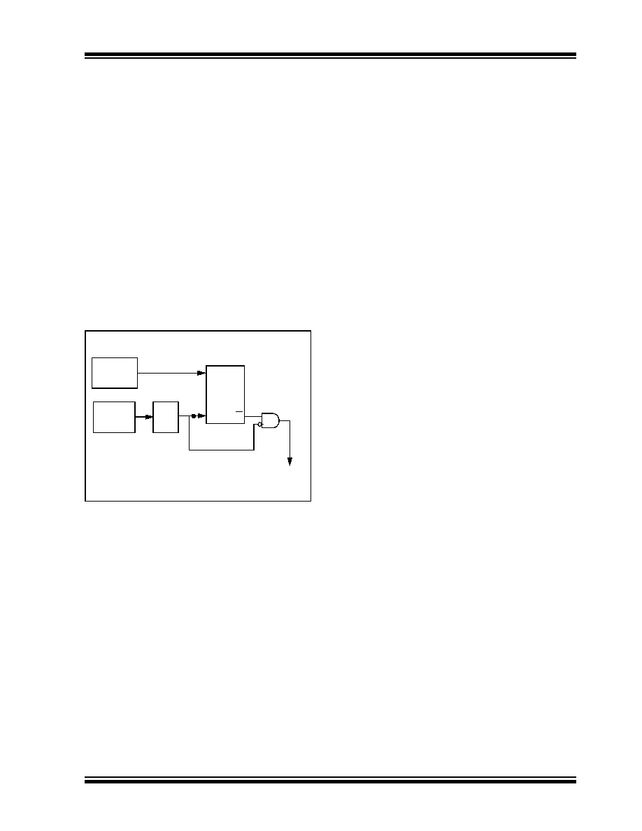
monitoring (shown in Figure 22-3) is accomplished by
creating a sample clock signal, which is the INTRC out-
put divided by 64. This allows ample time between
FSCM sample clocks for a peripheral clock edge to
occur. The peripheral device clock and the sample
clock are presented as inputs to the Clock Monitor latch
(CM). The CM is set on the falling edge of the device
clock source, but cleared on the rising edge of the
sample clock.
FIGURE 22-3:
FSCM BLOCK DIAGRAM
Clock failure is tested for on the falling edge of the
sample clock. If a sample clock falling edge occurs
while CM is still set, a clock failure has been detected
(Figure 22-4). This causes the following:
the FSCM generates an oscillator fail interrupt by
setting bit OSCFIF (PIR2<7>);
the device clock source is switched to the internal
oscillator block (OSCCON is not updated to show
the current clock source – this is the fail-safe
condition); and
the WDT is reset.
During switchover, the postscaler frequency from the
internal oscillator block may not be sufficiently stable
for timing sensitive applications. In these cases, it may
be desirable to select another clock configuration and
enter an alternate power-managed mode. This can be
done to attempt a partial recovery or execute a
controlled shutdown. See Section 3.1.4 “Multiple
more details.
To use a higher clock speed on wake-up, the INTOSC
or postscaler clock sources can be selected to provide
a higher clock speed by setting bits, IRCF2:IRCF0,
immediately after Reset. For wake-ups from Sleep, the
INTOSC or postscaler clock sources can be selected
by setting the IRCF2:IRCF0 bits prior to entering Sleep
mode.
The FSCM will detect failures of the primary or second-
ary clock sources only. If the internal oscillator block
fails, no failure would be detected, nor would any action
be possible.
22.4.1
FSCM AND THE WATCHDOG TIMER
Both the FSCM and the WDT are clocked by the
INTRC oscillator. Since the WDT operates with a
separate divider and counter, disabling the WDT has
no effect on the operation of the INTRC oscillator when
the FSCM is enabled.
As already noted, the clock source is switched to the
INTOSC clock when a clock failure is detected.
Depending on the frequency selected by the
IRCF2:IRCF0 bits, this may mean a substantial change
in the speed of code execution. If the WDT is enabled
with a small prescale value, a decrease in clock speed
allows a WDT time-out to occur and a subsequent
device Reset. For this reason, fail-safe clock events
also reset the WDT and postscaler, allowing it to start
timing from when execution speed was changed and
decreasing the likelihood of an erroneous time-out.
22.4.2
EXITING FAIL-SAFE OPERATION
The fail-safe condition is terminated by either a device
Reset or by entering a power-managed mode. On
Reset, the controller starts the primary clock source
specified in Configuration Register 1H (with any
required start-up delays that are required for the oscil-
lator mode, such as OST or PLL timer). The INTOSC
multiplexer provides the device clock until the primary
clock source becomes ready (similar to a Two-Speed
Start-up). The clock source is then switched to the pri-
mary clock (indicated by the OSTS bit in the OSCCON
register becoming set). The Fail-Safe Clock Monitor
then resumes monitoring the peripheral clock.
The primary clock source may never become ready
during start-up. In this case, operation is clocked by the
INTOSC multiplexer. The OSCCON register will remain
in its Reset state until a power-managed mode is
entered.
Peripheral
INTRC
÷ 64
S
C
Q
(32
μs)
488 Hz
(2.048 ms)
Clock Monitor
Latch (CM)
(edge-triggered)
Clock
Failure
Detected
Source
Clock
Q
相关PDF资料 |
PDF描述 |
|---|---|
| AT89LP4052-16SU | IC 8051 MCU FLASH 4K 20SOIC |
| PIC24FJ64GA106-I/MR | MCU PIC 64KB FLASH 64QFN |
| PIC18LF2510-I/SP | IC MCU FLASH 16KX16 28-DIP |
| PIC16C57-XTI/P | IC MCU OTP 2KX12 28DIP |
| ATMEGA88V-10PU | IC AVR MCU 8K 10MHZ 1.8V 28DIP |
相关代理商/技术参数 |
参数描述 |
|---|---|
| PIC16F747T-I/ML | 功能描述:8位微控制器 -MCU 7KB 368 RAM 36 I/O RoHS:否 制造商:Silicon Labs 核心:8051 处理器系列:C8051F39x 数据总线宽度:8 bit 最大时钟频率:50 MHz 程序存储器大小:16 KB 数据 RAM 大小:1 KB 片上 ADC:Yes 工作电源电压:1.8 V to 3.6 V 工作温度范围:- 40 C to + 105 C 封装 / 箱体:QFN-20 安装风格:SMD/SMT |
| PIC16F747T-I/PT | 功能描述:8位微控制器 -MCU 7KB 368 RAM 36 I/O RoHS:否 制造商:Silicon Labs 核心:8051 处理器系列:C8051F39x 数据总线宽度:8 bit 最大时钟频率:50 MHz 程序存储器大小:16 KB 数据 RAM 大小:1 KB 片上 ADC:Yes 工作电源电压:1.8 V to 3.6 V 工作温度范围:- 40 C to + 105 C 封装 / 箱体:QFN-20 安装风格:SMD/SMT |
| PIC16F74-E/L | 功能描述:8位微控制器 -MCU 7KB 192 RAM 33 I/O RoHS:否 制造商:Silicon Labs 核心:8051 处理器系列:C8051F39x 数据总线宽度:8 bit 最大时钟频率:50 MHz 程序存储器大小:16 KB 数据 RAM 大小:1 KB 片上 ADC:Yes 工作电源电压:1.8 V to 3.6 V 工作温度范围:- 40 C to + 105 C 封装 / 箱体:QFN-20 安装风格:SMD/SMT |
| PIC16F74-E/ML | 功能描述:8位微控制器 -MCU 7KB 192 RAM 33 I/O RoHS:否 制造商:Silicon Labs 核心:8051 处理器系列:C8051F39x 数据总线宽度:8 bit 最大时钟频率:50 MHz 程序存储器大小:16 KB 数据 RAM 大小:1 KB 片上 ADC:Yes 工作电源电压:1.8 V to 3.6 V 工作温度范围:- 40 C to + 105 C 封装 / 箱体:QFN-20 安装风格:SMD/SMT |
| PIC16F74-E/P | 功能描述:8位微控制器 -MCU 7KB 192 RAM 33 I/O RoHS:否 制造商:Silicon Labs 核心:8051 处理器系列:C8051F39x 数据总线宽度:8 bit 最大时钟频率:50 MHz 程序存储器大小:16 KB 数据 RAM 大小:1 KB 片上 ADC:Yes 工作电源电压:1.8 V to 3.6 V 工作温度范围:- 40 C to + 105 C 封装 / 箱体:QFN-20 安装风格:SMD/SMT |
发布紧急采购,3分钟左右您将得到回复。