- 您现在的位置:买卖IC网 > PDF目录11449 > PIC16F872-E/SS (Microchip Technology)IC MCU CMOS 20MHZ 2K FLSH 28SSOP PDF资料下载
参数资料
| 型号: | PIC16F872-E/SS |
| 厂商: | Microchip Technology |
| 文件页数: | 26/167页 |
| 文件大小: | 0K |
| 描述: | IC MCU CMOS 20MHZ 2K FLSH 28SSOP |
| 产品培训模块: | Asynchronous Stimulus |
| 标准包装: | 47 |
| 系列: | PIC® 16F |
| 核心处理器: | PIC |
| 芯体尺寸: | 8-位 |
| 速度: | 20MHz |
| 连通性: | I²C,SPI |
| 外围设备: | 欠压检测/复位,POR,PWM,WDT |
| 输入/输出数: | 22 |
| 程序存储器容量: | 3.5KB(2K x 14) |
| 程序存储器类型: | 闪存 |
| EEPROM 大小: | 64 x 8 |
| RAM 容量: | 128 x 8 |
| 电压 - 电源 (Vcc/Vdd): | 4 V ~ 5.5 V |
| 数据转换器: | A/D 5x10b |
| 振荡器型: | 外部 |
| 工作温度: | -40°C ~ 125°C |
| 封装/外壳: | 28-SSOP(0.209",5.30mm 宽) |
| 包装: | 管件 |
第1页第2页第3页第4页第5页第6页第7页第8页第9页第10页第11页第12页第13页第14页第15页第16页第17页第18页第19页第20页第21页第22页第23页第24页第25页当前第26页第27页第28页第29页第30页第31页第32页第33页第34页第35页第36页第37页第38页第39页第40页第41页第42页第43页第44页第45页第46页第47页第48页第49页第50页第51页第52页第53页第54页第55页第56页第57页第58页第59页第60页第61页第62页第63页第64页第65页第66页第67页第68页第69页第70页第71页第72页第73页第74页第75页第76页第77页第78页第79页第80页第81页第82页第83页第84页第85页第86页第87页第88页第89页第90页第91页第92页第93页第94页第95页第96页第97页第98页第99页第100页第101页第102页第103页第104页第105页第106页第107页第108页第109页第110页第111页第112页第113页第114页第115页第116页第117页第118页第119页第120页第121页第122页第123页第124页第125页第126页第127页第128页第129页第130页第131页第132页第133页第134页第135页第136页第137页第138页第139页第140页第141页第142页第143页第144页第145页第146页第147页第148页第149页第150页第151页第152页第153页第154页第155页第156页第157页第158页第159页第160页第161页第162页第163页第164页第165页第166页第167页
122
8048C–AVR–02/12
ATtiny43U
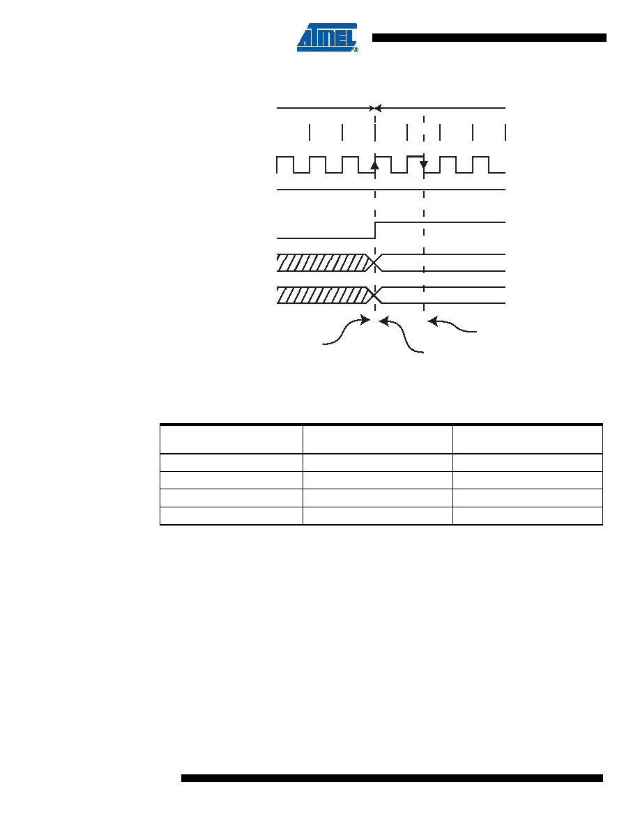
Figure 16-7. ADC Timing Diagram, Free Running Conversion
For a summary of conversion times, see Table 16-1.
16.6
Changing Channel or Reference Selection
The MUX[2:0] and REFS bits in the ADMUX Register are single buffered through a temporary
register to which the CPU has random access. This ensures that the channels and reference
selection only takes place at a safe point during the conversion. The channel and reference
selection is continuously updated until a conversion is started. Once the conversion starts, the
channel and reference selection is locked to ensure a sufficient sampling time for the ADC. Con-
tinuous updating resumes in the last ADC clock cycle before the conversion completes (ADIF in
ADCSRA is set). Note that the conversion starts on the following rising ADC clock edge after
ADSC is written. The user is thus advised not to write new channel or reference selection values
to ADMUX until one ADC clock cycle after ADSC is written.
If Auto Triggering is used, the exact time of the triggering event can be indeterministic. Special
care must be taken when updating the ADMUX Register, in order to control which conversion
will be affected by the new settings.
Table 16-1.
ADC Conversion Time
Condition
Sample & Hold (Cycles from
Start of Conversion)
Conversion Time (Cycles)
First conversion
13.5
25
Normal conversions
1.5
13
Auto Triggered conversions
2
13.5
Free Running conversion
2.5
14
11
12
13
Sign and MSB of Result
LSB of Result
ADC Clock
ADSC
ADIF
ADCH
ADCL
Cycle Number
12
One Conversion
Next Conversion
34
Conversion
Complete
Sample & Hold
MUX and REFS
Update
相关PDF资料 |
PDF描述 |
|---|---|
| VI-J4N-IY-B1 | CONVERTER MOD DC/DC 18.5V 50W |
| SN74LV4066ADBR | IC SWITCH QUAD 1X1 14SSOP |
| VE-J5N-IY-B1 | CONVERTER MOD DC/DC 18.5V 50W |
| VE-BND-IX-S | CONVERTER MOD DC/DC 85V 75W |
| PIC18F4321-E/ML | IC PIC MCU FLASH 4KX16 44QFN |
相关代理商/技术参数 |
参数描述 |
|---|---|
| PIC16F872-I/SO | 功能描述:8位微控制器 -MCU 3.5KB 128 RAM 22 I/O RoHS:否 制造商:Silicon Labs 核心:8051 处理器系列:C8051F39x 数据总线宽度:8 bit 最大时钟频率:50 MHz 程序存储器大小:16 KB 数据 RAM 大小:1 KB 片上 ADC:Yes 工作电源电压:1.8 V to 3.6 V 工作温度范围:- 40 C to + 105 C 封装 / 箱体:QFN-20 安装风格:SMD/SMT |
| PIC16F872-I/SO | 制造商:Microchip Technology Inc 功能描述:8BIT FLASH MCU SMD 16F872 SOIC28 |
| PIC16F872-I/SOG | 功能描述:8位微控制器 -MCU 3.5KB 128 RAM 22 I/O Lead Free Package RoHS:否 制造商:Silicon Labs 核心:8051 处理器系列:C8051F39x 数据总线宽度:8 bit 最大时钟频率:50 MHz 程序存储器大小:16 KB 数据 RAM 大小:1 KB 片上 ADC:Yes 工作电源电压:1.8 V to 3.6 V 工作温度范围:- 40 C to + 105 C 封装 / 箱体:QFN-20 安装风格:SMD/SMT |
| PIC16F872-I/SP | 功能描述:8位微控制器 -MCU 3.5KB 128 RAM 22 I/O RoHS:否 制造商:Silicon Labs 核心:8051 处理器系列:C8051F39x 数据总线宽度:8 bit 最大时钟频率:50 MHz 程序存储器大小:16 KB 数据 RAM 大小:1 KB 片上 ADC:Yes 工作电源电压:1.8 V to 3.6 V 工作温度范围:- 40 C to + 105 C 封装 / 箱体:QFN-20 安装风格:SMD/SMT |
| PIC16F872-I/SP | 制造商:Microchip Technology Inc 功能描述:IC 8BIT FLASH MCU 16F872 SDIL28 |
发布紧急采购,3分钟左右您将得到回复。