- 您现在的位置:买卖IC网 > PDF目录11449 > PIC16F872-E/SS (Microchip Technology)IC MCU CMOS 20MHZ 2K FLSH 28SSOP PDF资料下载
参数资料
| 型号: | PIC16F872-E/SS |
| 厂商: | Microchip Technology |
| 文件页数: | 6/167页 |
| 文件大小: | 0K |
| 描述: | IC MCU CMOS 20MHZ 2K FLSH 28SSOP |
| 产品培训模块: | Asynchronous Stimulus |
| 标准包装: | 47 |
| 系列: | PIC® 16F |
| 核心处理器: | PIC |
| 芯体尺寸: | 8-位 |
| 速度: | 20MHz |
| 连通性: | I²C,SPI |
| 外围设备: | 欠压检测/复位,POR,PWM,WDT |
| 输入/输出数: | 22 |
| 程序存储器容量: | 3.5KB(2K x 14) |
| 程序存储器类型: | 闪存 |
| EEPROM 大小: | 64 x 8 |
| RAM 容量: | 128 x 8 |
| 电压 - 电源 (Vcc/Vdd): | 4 V ~ 5.5 V |
| 数据转换器: | A/D 5x10b |
| 振荡器型: | 外部 |
| 工作温度: | -40°C ~ 125°C |
| 封装/外壳: | 28-SSOP(0.209",5.30mm 宽) |
| 包装: | 管件 |
第1页第2页第3页第4页第5页当前第6页第7页第8页第9页第10页第11页第12页第13页第14页第15页第16页第17页第18页第19页第20页第21页第22页第23页第24页第25页第26页第27页第28页第29页第30页第31页第32页第33页第34页第35页第36页第37页第38页第39页第40页第41页第42页第43页第44页第45页第46页第47页第48页第49页第50页第51页第52页第53页第54页第55页第56页第57页第58页第59页第60页第61页第62页第63页第64页第65页第66页第67页第68页第69页第70页第71页第72页第73页第74页第75页第76页第77页第78页第79页第80页第81页第82页第83页第84页第85页第86页第87页第88页第89页第90页第91页第92页第93页第94页第95页第96页第97页第98页第99页第100页第101页第102页第103页第104页第105页第106页第107页第108页第109页第110页第111页第112页第113页第114页第115页第116页第117页第118页第119页第120页第121页第122页第123页第124页第125页第126页第127页第128页第129页第130页第131页第132页第133页第134页第135页第136页第137页第138页第139页第140页第141页第142页第143页第144页第145页第146页第147页第148页第149页第150页第151页第152页第153页第154页第155页第156页第157页第158页第159页第160页第161页第162页第163页第164页第165页第166页第167页
103
8048C–AVR–02/12
ATtiny43U
output to the opposite clock edge of the data input sampling. The serial input is always sampled
from the Data Input (DI) pin independent of the configuration.
The 4-bit counter can be both read and written via the data bus, and it can generate an overflow
interrupt. Both the USI Data Register and the counter are clocked simultaneously by the same
clock source. This allows the counter to count the number of bits received or transmitted and
generate an interrupt when the transfer is complete. Note that when an external clock source is
selected the counter counts both clock edges. This means the counter registers the number of
clock edges and not the number of data bits. The clock can be selected from three different
sources: The USCK pin, Timer/Counter0 Compare Match or from software.
The two-wire clock control unit can be configured to generate an interrupt when a start condition
has been detected on the two-wire bus. It can also be set to generate wait states by holding the
clock pin low after a start condition is detected, or after the counter overflows.
14.3
Functional Descriptions
14.3.1
Three-wire Mode
The USI Three-wire mode is compliant to the Serial Peripheral Interface (SPI) mode 0 and 1, but
does not have the slave select (SS) pin functionality. However, this feature can be implemented
in software if necessary. Pin names used by this mode are: DI, DO, and USCK.
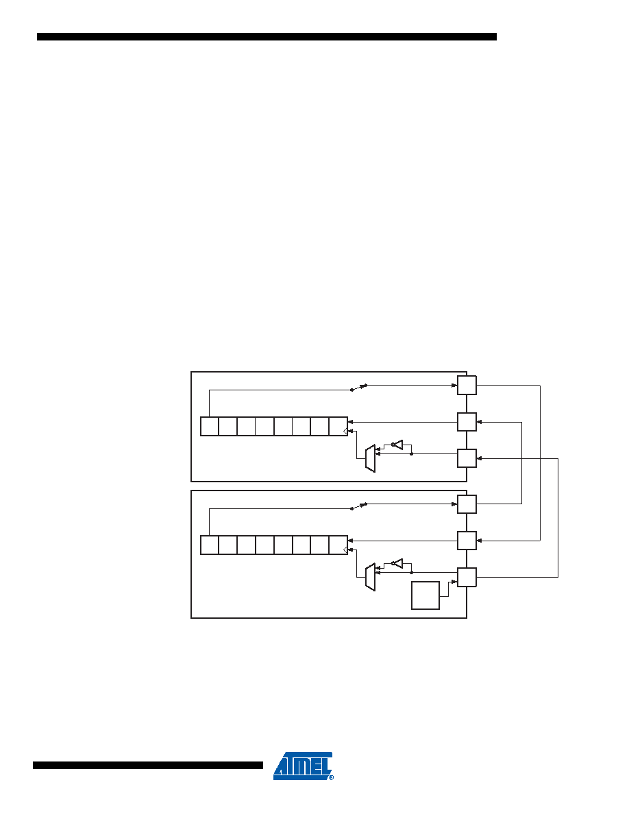
Figure 14-2. Three-wire Mode Operation, Simplified Diagram
Figure 14-2 shows two USI units operating in three-wire mode, one as Master and one as Slave.
The two USI Data Registers are interconnected in such way that after eight USCK clocks, the
data in each register has been interchanged. The same clock also increments the USI’s 4-bit
counter. The Counter Overflow (interrupt) Flag, or USIOIF, can therefore be used to determine
when a transfer is completed. The clock is generated by the Master device software by toggling
the USCK pin via the PORTA register or by writing a one to bit USITC bit in USICR.
SLAVE
MASTER
Bit7
Bit6
Bit5
Bit4
Bit3
Bit2
Bit1
Bit0
DO
DI
USCK
Bit7
Bit6
Bit5
Bit4
Bit3
Bit2
Bit1
Bit0
DO
DI
USCK
PORTxn
相关PDF资料 |
PDF描述 |
|---|---|
| VI-J4N-IY-B1 | CONVERTER MOD DC/DC 18.5V 50W |
| SN74LV4066ADBR | IC SWITCH QUAD 1X1 14SSOP |
| VE-J5N-IY-B1 | CONVERTER MOD DC/DC 18.5V 50W |
| VE-BND-IX-S | CONVERTER MOD DC/DC 85V 75W |
| PIC18F4321-E/ML | IC PIC MCU FLASH 4KX16 44QFN |
相关代理商/技术参数 |
参数描述 |
|---|---|
| PIC16F872-I/SO | 功能描述:8位微控制器 -MCU 3.5KB 128 RAM 22 I/O RoHS:否 制造商:Silicon Labs 核心:8051 处理器系列:C8051F39x 数据总线宽度:8 bit 最大时钟频率:50 MHz 程序存储器大小:16 KB 数据 RAM 大小:1 KB 片上 ADC:Yes 工作电源电压:1.8 V to 3.6 V 工作温度范围:- 40 C to + 105 C 封装 / 箱体:QFN-20 安装风格:SMD/SMT |
| PIC16F872-I/SO | 制造商:Microchip Technology Inc 功能描述:8BIT FLASH MCU SMD 16F872 SOIC28 |
| PIC16F872-I/SOG | 功能描述:8位微控制器 -MCU 3.5KB 128 RAM 22 I/O Lead Free Package RoHS:否 制造商:Silicon Labs 核心:8051 处理器系列:C8051F39x 数据总线宽度:8 bit 最大时钟频率:50 MHz 程序存储器大小:16 KB 数据 RAM 大小:1 KB 片上 ADC:Yes 工作电源电压:1.8 V to 3.6 V 工作温度范围:- 40 C to + 105 C 封装 / 箱体:QFN-20 安装风格:SMD/SMT |
| PIC16F872-I/SP | 功能描述:8位微控制器 -MCU 3.5KB 128 RAM 22 I/O RoHS:否 制造商:Silicon Labs 核心:8051 处理器系列:C8051F39x 数据总线宽度:8 bit 最大时钟频率:50 MHz 程序存储器大小:16 KB 数据 RAM 大小:1 KB 片上 ADC:Yes 工作电源电压:1.8 V to 3.6 V 工作温度范围:- 40 C to + 105 C 封装 / 箱体:QFN-20 安装风格:SMD/SMT |
| PIC16F872-I/SP | 制造商:Microchip Technology Inc 功能描述:IC 8BIT FLASH MCU 16F872 SDIL28 |
发布紧急采购,3分钟左右您将得到回复。