- 您现在的位置:买卖IC网 > PDF目录11538 > PIC16F913T-I/SO (Microchip Technology)IC PIC MCU FLASH 4KX14 28SOIC PDF资料下载
参数资料
| 型号: | PIC16F913T-I/SO |
| 厂商: | Microchip Technology |
| 文件页数: | 39/229页 |
| 文件大小: | 0K |
| 描述: | IC PIC MCU FLASH 4KX14 28SOIC |
| 产品培训模块: | Asynchronous Stimulus |
| 标准包装: | 1,600 |
| 系列: | PIC® 16F |
| 核心处理器: | PIC |
| 芯体尺寸: | 8-位 |
| 速度: | 20MHz |
| 连通性: | I²C,SPI,UART/USART |
| 外围设备: | 欠压检测/复位,LCD,POR,PWM,WDT |
| 输入/输出数: | 24 |
| 程序存储器容量: | 7KB(4K x 14) |
| 程序存储器类型: | 闪存 |
| EEPROM 大小: | 256 x 8 |
| RAM 容量: | 256 x 8 |
| 电压 - 电源 (Vcc/Vdd): | 2 V ~ 5.5 V |
| 数据转换器: | A/D 5x10b |
| 振荡器型: | 内部 |
| 工作温度: | -40°C ~ 85°C |
| 封装/外壳: | 28-SOIC(0.295",7.50mm 宽) |
| 包装: | 带卷 (TR) |
第1页第2页第3页第4页第5页第6页第7页第8页第9页第10页第11页第12页第13页第14页第15页第16页第17页第18页第19页第20页第21页第22页第23页第24页第25页第26页第27页第28页第29页第30页第31页第32页第33页第34页第35页第36页第37页第38页当前第39页第40页第41页第42页第43页第44页第45页第46页第47页第48页第49页第50页第51页第52页第53页第54页第55页第56页第57页第58页第59页第60页第61页第62页第63页第64页第65页第66页第67页第68页第69页第70页第71页第72页第73页第74页第75页第76页第77页第78页第79页第80页第81页第82页第83页第84页第85页第86页第87页第88页第89页第90页第91页第92页第93页第94页第95页第96页第97页第98页第99页第100页第101页第102页第103页第104页第105页第106页第107页第108页第109页第110页第111页第112页第113页第114页第115页第116页第117页第118页第119页第120页第121页第122页第123页第124页第125页第126页第127页第128页第129页第130页第131页第132页第133页第134页第135页第136页第137页第138页第139页第140页第141页第142页第143页第144页第145页第146页第147页第148页第149页第150页第151页第152页第153页第154页第155页第156页第157页第158页第159页第160页第161页第162页第163页第164页第165页第166页第167页第168页第169页第170页第171页第172页第173页第174页第175页第176页第177页第178页第179页第180页第181页第182页第183页第184页第185页第186页第187页第188页第189页第190页第191页第192页第193页第194页第195页第196页第197页第198页第199页第200页第201页第202页第203页第204页第205页第206页第207页第208页第209页第210页第211页第212页第213页第214页第215页第216页第217页第218页第219页第220页第221页第222页第223页第224页第225页第226页第227页第228页第229页
218
8018P–AVR–08/10
ATmega169P
If the result is left adjusted and no more than 8-bit precision is required, it is sufficient to read
ADCH. Otherwise, ADCL must be read first, then ADCH, to ensure that the content of the Data
Registers belongs to the same conversion. Once ADCL is read, ADC access to Data Registers
is blocked. This means that if ADCL has been read, and a conversion completes before ADCH is
read, neither register is updated and the result from the conversion is lost. When ADCH is read,
ADC access to the ADCH and ADCL Registers is re-enabled.
The ADC has its own interrupt which can be triggered when a conversion completes. When ADC
access to the Data Registers is prohibited between reading of ADCH and ADCL, the interrupt
will trigger even if the result is lost.
22.4
Starting a Conversion
A single conversion is started by writing a logical one to the ADC Start Conversion bit, ADSC.
This bit stays high as long as the conversion is in progress and will be cleared by hardware
when the conversion is completed. If a different data channel is selected while a conversion is in
progress, the ADC will finish the current conversion before performing the channel change.
Alternatively, a conversion can be triggered automatically by various sources. Auto Triggering is
enabled by setting the ADC Auto Trigger Enable bit, ADATE in ADCSRA. The trigger source is
selected by setting the ADC Trigger Select bits, ADTS in ADCSRB (See description of the ADTS
bits for a list of the trigger sources). When a positive edge occurs on the selected trigger signal,
the ADC prescaler is reset and a conversion is started. This provides a method of starting con-
versions at fixed intervals. If the trigger signal still is set when the conversion completes, a new
conversion will not be started. If another positive edge occurs on the trigger signal during con-
version, the edge will be ignored. Note that an Interrupt Flag will be set even if the specific
interrupt is disabled or the Global Interrupt Enable bit in SREG is cleared. A conversion can thus
be triggered without causing an interrupt. However, the Interrupt Flag must be cleared in order to
trigger a new conversion at the next interrupt event.
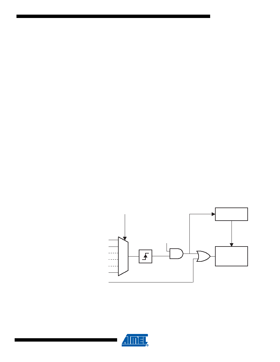
Figure 22-2. ADC Auto Trigger Logic
Using the ADC Interrupt Flag as a trigger source makes the ADC start a new conversion as soon
as the ongoing conversion has finished. The ADC then operates in Free Running mode, con-
stantly sampling and updating the ADC Data Register. The first conversion must be started by
writing a logical one to the ADSC bit in ADCSRA. In this mode the ADC will perform successive
conversions independently of whether the ADC Interrupt Flag, ADIF is cleared or not.
ADSC
ADIF
SOURCE 1
SOURCE n
ADTS[2:0]
CONVERSION
LOGIC
PRESCALER
START
CLK
ADC
.
EDGE
DETECTOR
ADATE
相关PDF资料 |
PDF描述 |
|---|---|
| VE-2WZ-IX-B1 | CONVERTER MOD DC/DC 2V 30W |
| VE-2WZ-IW-B1 | CONVERTER MOD DC/DC 2V 40W |
| VE-2WY-IX-B1 | CONVERTER MOD DC/DC 3.3V 49.5W |
| 112434 | CONN ADPT BNC JACK-JACK BULKHEAD |
| VE-2WY-IW-B1 | CONVERTER MOD DC/DC 3.3V 66W |
相关代理商/技术参数 |
参数描述 |
|---|---|
| PIC16F914-E/ML | 功能描述:8位微控制器 -MCU 7KB FL 352R 36 I/O RoHS:否 制造商:Silicon Labs 核心:8051 处理器系列:C8051F39x 数据总线宽度:8 bit 最大时钟频率:50 MHz 程序存储器大小:16 KB 数据 RAM 大小:1 KB 片上 ADC:Yes 工作电源电压:1.8 V to 3.6 V 工作温度范围:- 40 C to + 105 C 封装 / 箱体:QFN-20 安装风格:SMD/SMT |
| PIC16F914-E/P | 功能描述:8位微控制器 -MCU 7KB FL 352R 36 I/O RoHS:否 制造商:Silicon Labs 核心:8051 处理器系列:C8051F39x 数据总线宽度:8 bit 最大时钟频率:50 MHz 程序存储器大小:16 KB 数据 RAM 大小:1 KB 片上 ADC:Yes 工作电源电压:1.8 V to 3.6 V 工作温度范围:- 40 C to + 105 C 封装 / 箱体:QFN-20 安装风格:SMD/SMT |
| PIC16F914-E/PT | 功能描述:8位微控制器 -MCU 7KB FL 352R 36 I/O RoHS:否 制造商:Silicon Labs 核心:8051 处理器系列:C8051F39x 数据总线宽度:8 bit 最大时钟频率:50 MHz 程序存储器大小:16 KB 数据 RAM 大小:1 KB 片上 ADC:Yes 工作电源电压:1.8 V to 3.6 V 工作温度范围:- 40 C to + 105 C 封装 / 箱体:QFN-20 安装风格:SMD/SMT |
| PIC16F914-I/ML | 功能描述:8位微控制器 -MCU 7KB FL 352R 36 I/O RoHS:否 制造商:Silicon Labs 核心:8051 处理器系列:C8051F39x 数据总线宽度:8 bit 最大时钟频率:50 MHz 程序存储器大小:16 KB 数据 RAM 大小:1 KB 片上 ADC:Yes 工作电源电压:1.8 V to 3.6 V 工作温度范围:- 40 C to + 105 C 封装 / 箱体:QFN-20 安装风格:SMD/SMT |
| PIC16F914-I/P | 功能描述:8位微控制器 -MCU 7KB FL 352R 36 I/O RoHS:否 制造商:Silicon Labs 核心:8051 处理器系列:C8051F39x 数据总线宽度:8 bit 最大时钟频率:50 MHz 程序存储器大小:16 KB 数据 RAM 大小:1 KB 片上 ADC:Yes 工作电源电压:1.8 V to 3.6 V 工作温度范围:- 40 C to + 105 C 封装 / 箱体:QFN-20 安装风格:SMD/SMT |
发布紧急采购,3分钟左右您将得到回复。