- 您现在的位置:买卖IC网 > PDF目录11538 > PIC16F913T-I/SO (Microchip Technology)IC PIC MCU FLASH 4KX14 28SOIC PDF资料下载
参数资料
| 型号: | PIC16F913T-I/SO |
| 厂商: | Microchip Technology |
| 文件页数: | 59/229页 |
| 文件大小: | 0K |
| 描述: | IC PIC MCU FLASH 4KX14 28SOIC |
| 产品培训模块: | Asynchronous Stimulus |
| 标准包装: | 1,600 |
| 系列: | PIC® 16F |
| 核心处理器: | PIC |
| 芯体尺寸: | 8-位 |
| 速度: | 20MHz |
| 连通性: | I²C,SPI,UART/USART |
| 外围设备: | 欠压检测/复位,LCD,POR,PWM,WDT |
| 输入/输出数: | 24 |
| 程序存储器容量: | 7KB(4K x 14) |
| 程序存储器类型: | 闪存 |
| EEPROM 大小: | 256 x 8 |
| RAM 容量: | 256 x 8 |
| 电压 - 电源 (Vcc/Vdd): | 2 V ~ 5.5 V |
| 数据转换器: | A/D 5x10b |
| 振荡器型: | 内部 |
| 工作温度: | -40°C ~ 85°C |
| 封装/外壳: | 28-SOIC(0.295",7.50mm 宽) |
| 包装: | 带卷 (TR) |
第1页第2页第3页第4页第5页第6页第7页第8页第9页第10页第11页第12页第13页第14页第15页第16页第17页第18页第19页第20页第21页第22页第23页第24页第25页第26页第27页第28页第29页第30页第31页第32页第33页第34页第35页第36页第37页第38页第39页第40页第41页第42页第43页第44页第45页第46页第47页第48页第49页第50页第51页第52页第53页第54页第55页第56页第57页第58页当前第59页第60页第61页第62页第63页第64页第65页第66页第67页第68页第69页第70页第71页第72页第73页第74页第75页第76页第77页第78页第79页第80页第81页第82页第83页第84页第85页第86页第87页第88页第89页第90页第91页第92页第93页第94页第95页第96页第97页第98页第99页第100页第101页第102页第103页第104页第105页第106页第107页第108页第109页第110页第111页第112页第113页第114页第115页第116页第117页第118页第119页第120页第121页第122页第123页第124页第125页第126页第127页第128页第129页第130页第131页第132页第133页第134页第135页第136页第137页第138页第139页第140页第141页第142页第143页第144页第145页第146页第147页第148页第149页第150页第151页第152页第153页第154页第155页第156页第157页第158页第159页第160页第161页第162页第163页第164页第165页第166页第167页第168页第169页第170页第171页第172页第173页第174页第175页第176页第177页第178页第179页第180页第181页第182页第183页第184页第185页第186页第187页第188页第189页第190页第191页第192页第193页第194页第195页第196页第197页第198页第199页第200页第201页第202页第203页第204页第205页第206页第207页第208页第209页第210页第211页第212页第213页第214页第215页第216页第217页第218页第219页第220页第221页第222页第223页第224页第225页第226页第227页第228页第229页
236
8018P–AVR–08/10
ATmega169P
To energize a segment, an absolute voltage above a certain threshold must be applied. This is
done by letting the output voltage on corresponding COM pin and SEG pin have opposite phase.
For display with more than one common, one (1/2 bias) or two (1/3 bias) additional voltage lev-
els must be applied. Otherwise, non-energized segments on COM0 would be energized for all
non-selected common.
Addressing COM0 starts a frame by driving opposite phase with large amplitude out on COM0
compared to none addressed COM lines. Non-energized segments are in phase with the
addressed COM0, and energized segments have opposite phase and large amplitude. For
waveform figures refer to ”Mode of Operation” on page 237. Latched data from LCDDR4 -
LCDDR0 is multiplexed into the decoder. The decoder is controlled from the LCD timing and
sets up signals controlling the analog switches to produce an output waveform. Next, COM1 is
addressed, and latched data from LCDDR9 - LCDDR5 is input to decoder. Addressing continu-
ous until all COM lines are addressed according to number of common (duty). The display data
are latched before a new frame start.
23.2.5
LCD Contrast Controller/Power Supply
The peak value (V
LCD) on the output waveform determines the LCD Contrast. VLCD is controlled
by software from 2.6V to 3.35V independent of V
CC. An internal signal inhibits output to the LCD
until V
LCD has reached its target value.
23.2.6
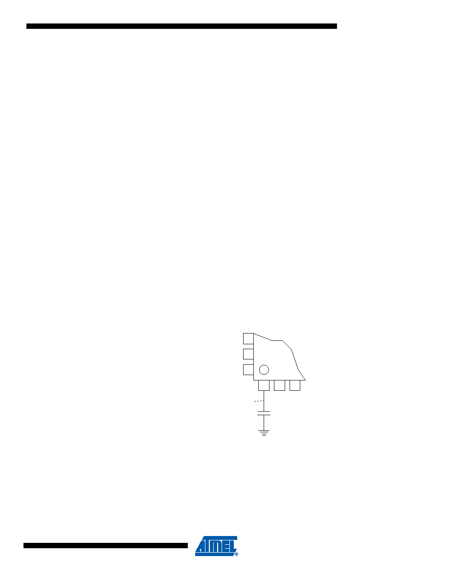
LCDCAP
An external capacitor (typical > 470 nF) must be connected to the LCDCAP pin as shown in Fig-
ure 23-2. This capacitor acts as a reservoir for LCD power (V
LCD). A large capacitance reduces
ripple on V
LCD but increases the time until VLCD reaches its target value.
It is possible to use an external power supply. This power can be applied to LCDCAP before
V
CC. Externally applied VLCD can be both above and below VCC. Maximum VLCD is 5.5V.
Figure 23-2. LCDCAP Connection
23.2.7
LCD Buffer Driver
Intermediate voltage levels are generated from buffers/drivers. The buffers are active the
amount of time specified by LCDDC[2:0] in ”LCDCCR – LCD Contrast Control Register” on page
250. Then LCD output pins are tri-stated and buffers are switched off. Shortening the drive time
will reduce power consumption, but displays with high internal resistance or capacitance may
need longer drive time to achieve sufficient contrast.
3
2
1
64
63
62
LCDCAP
V
LCD
(Optional)
相关PDF资料 |
PDF描述 |
|---|---|
| VE-2WZ-IX-B1 | CONVERTER MOD DC/DC 2V 30W |
| VE-2WZ-IW-B1 | CONVERTER MOD DC/DC 2V 40W |
| VE-2WY-IX-B1 | CONVERTER MOD DC/DC 3.3V 49.5W |
| 112434 | CONN ADPT BNC JACK-JACK BULKHEAD |
| VE-2WY-IW-B1 | CONVERTER MOD DC/DC 3.3V 66W |
相关代理商/技术参数 |
参数描述 |
|---|---|
| PIC16F914-E/ML | 功能描述:8位微控制器 -MCU 7KB FL 352R 36 I/O RoHS:否 制造商:Silicon Labs 核心:8051 处理器系列:C8051F39x 数据总线宽度:8 bit 最大时钟频率:50 MHz 程序存储器大小:16 KB 数据 RAM 大小:1 KB 片上 ADC:Yes 工作电源电压:1.8 V to 3.6 V 工作温度范围:- 40 C to + 105 C 封装 / 箱体:QFN-20 安装风格:SMD/SMT |
| PIC16F914-E/P | 功能描述:8位微控制器 -MCU 7KB FL 352R 36 I/O RoHS:否 制造商:Silicon Labs 核心:8051 处理器系列:C8051F39x 数据总线宽度:8 bit 最大时钟频率:50 MHz 程序存储器大小:16 KB 数据 RAM 大小:1 KB 片上 ADC:Yes 工作电源电压:1.8 V to 3.6 V 工作温度范围:- 40 C to + 105 C 封装 / 箱体:QFN-20 安装风格:SMD/SMT |
| PIC16F914-E/PT | 功能描述:8位微控制器 -MCU 7KB FL 352R 36 I/O RoHS:否 制造商:Silicon Labs 核心:8051 处理器系列:C8051F39x 数据总线宽度:8 bit 最大时钟频率:50 MHz 程序存储器大小:16 KB 数据 RAM 大小:1 KB 片上 ADC:Yes 工作电源电压:1.8 V to 3.6 V 工作温度范围:- 40 C to + 105 C 封装 / 箱体:QFN-20 安装风格:SMD/SMT |
| PIC16F914-I/ML | 功能描述:8位微控制器 -MCU 7KB FL 352R 36 I/O RoHS:否 制造商:Silicon Labs 核心:8051 处理器系列:C8051F39x 数据总线宽度:8 bit 最大时钟频率:50 MHz 程序存储器大小:16 KB 数据 RAM 大小:1 KB 片上 ADC:Yes 工作电源电压:1.8 V to 3.6 V 工作温度范围:- 40 C to + 105 C 封装 / 箱体:QFN-20 安装风格:SMD/SMT |
| PIC16F914-I/P | 功能描述:8位微控制器 -MCU 7KB FL 352R 36 I/O RoHS:否 制造商:Silicon Labs 核心:8051 处理器系列:C8051F39x 数据总线宽度:8 bit 最大时钟频率:50 MHz 程序存储器大小:16 KB 数据 RAM 大小:1 KB 片上 ADC:Yes 工作电源电压:1.8 V to 3.6 V 工作温度范围:- 40 C to + 105 C 封装 / 箱体:QFN-20 安装风格:SMD/SMT |
发布紧急采购,3分钟左右您将得到回复。