- 您现在的位置:买卖IC网 > PDF目录11481 > PIC16F946T-I/PT (Microchip Technology)IC PIC MCU FLASH 8KX14 64TQFP PDF资料下载
参数资料
| 型号: | PIC16F946T-I/PT |
| 厂商: | Microchip Technology |
| 文件页数: | 180/274页 |
| 文件大小: | 0K |
| 描述: | IC PIC MCU FLASH 8KX14 64TQFP |
| 产品培训模块: | Asynchronous Stimulus |
| 标准包装: | 1,200 |
| 系列: | PIC® 16F |
| 核心处理器: | PIC |
| 芯体尺寸: | 8-位 |
| 速度: | 20MHz |
| 连通性: | I²C,SPI,UART/USART |
| 外围设备: | 欠压检测/复位,LCD,POR,PWM,WDT |
| 输入/输出数: | 53 |
| 程序存储器容量: | 14KB(8K x 14) |
| 程序存储器类型: | 闪存 |
| EEPROM 大小: | 256 x 8 |
| RAM 容量: | 336 x 8 |
| 电压 - 电源 (Vcc/Vdd): | 2 V ~ 5.5 V |
| 数据转换器: | A/D 8x10b |
| 振荡器型: | 内部 |
| 工作温度: | -40°C ~ 85°C |
| 封装/外壳: | 64-TQFP |
| 包装: | 带卷 (TR) |
| 配用: | MA160011-ND - DAUGHTER BOARD PICDEM LCD 16F91X |
第1页第2页第3页第4页第5页第6页第7页第8页第9页第10页第11页第12页第13页第14页第15页第16页第17页第18页第19页第20页第21页第22页第23页第24页第25页第26页第27页第28页第29页第30页第31页第32页第33页第34页第35页第36页第37页第38页第39页第40页第41页第42页第43页第44页第45页第46页第47页第48页第49页第50页第51页第52页第53页第54页第55页第56页第57页第58页第59页第60页第61页第62页第63页第64页第65页第66页第67页第68页第69页第70页第71页第72页第73页第74页第75页第76页第77页第78页第79页第80页第81页第82页第83页第84页第85页第86页第87页第88页第89页第90页第91页第92页第93页第94页第95页第96页第97页第98页第99页第100页第101页第102页第103页第104页第105页第106页第107页第108页第109页第110页第111页第112页第113页第114页第115页第116页第117页第118页第119页第120页第121页第122页第123页第124页第125页第126页第127页第128页第129页第130页第131页第132页第133页第134页第135页第136页第137页第138页第139页第140页第141页第142页第143页第144页第145页第146页第147页第148页第149页第150页第151页第152页第153页第154页第155页第156页第157页第158页第159页第160页第161页第162页第163页第164页第165页第166页第167页第168页第169页第170页第171页第172页第173页第174页第175页第176页第177页第178页第179页当前第180页第181页第182页第183页第184页第185页第186页第187页第188页第189页第190页第191页第192页第193页第194页第195页第196页第197页第198页第199页第200页第201页第202页第203页第204页第205页第206页第207页第208页第209页第210页第211页第212页第213页第214页第215页第216页第217页第218页第219页第220页第221页第222页第223页第224页第225页第226页第227页第228页第229页第230页第231页第232页第233页第234页第235页第236页第237页第238页第239页第240页第241页第242页第243页第244页第245页第246页第247页第248页第249页第250页第251页第252页第253页第254页第255页第256页第257页第258页第259页第260页第261页第262页第263页第264页第265页第266页第267页第268页第269页第270页第271页第272页第273页第274页
260
8154B–AVR–07/09
ATmega16A
the value of the Fuse High bits (FHB) will be loaded in the destination register as shown below.
Refer to Table 26-3 on page 265 for detailed description and mapping of the Fuse High bits.
Fuse and Lock bits that are programmed, will be read as zero. Fuse and Lock bits that are
unprogrammed, will be read as one.
25.8.10
Preventing Flash Corruption
During periods of low V
CC, the Flash program can be corrupted because the supply voltage is too
low for the CPU and the Flash to operate properly. These issues are the same as for board level
systems using the Flash, and the same design solutions should be applied.
A Flash program corruption can be caused by two situations when the voltage is too low. First, a
regular write sequence to the Flash requires a minimum voltage to operate correctly. Secondly,
the CPU itself can execute instructions incorrectly, if the supply voltage for executing instructions
is too low.
Flash corruption can easily be avoided by following these design recommendations (one is
sufficient):
1.
If there is no need for a Boot Loader update in the system, program the Boot Loader
Lock bits to prevent any Boot Loader software updates.
2.
Keep the AVR RESET active (low) during periods of insufficient power supply voltage.
This can be done by enabling the internal Brown-out Detector (BOD) if the operating
voltage matches the detection level. If not, an external low V
CC Reset Protection circuit
can be used. If a reset occurs while a write operation is in progress, the write operation
will be completed provided that the power supply voltage is sufficient.
3.
Keep the AVR core in Power-down Sleep mode during periods of low V
CC. This will pre-
vent the CPU from attempting to decode and execute instructions, effectively protecting
the SPMCR Register and thus the Flash from unintentional writes.
25.8.11
Programming Time for Flash when using SPM
The Calibrated RC Oscillator is used to time Flash accesses. Table 25-5 shows the typical pro-
gramming time for Flash accesses from the CPU.
25.8.12
Simple Assembly Code Example for a Boot Loader
;-the routine writes one page of data from RAM to Flash
; the first data location in RAM is pointed to by the Y pointer
; the first data location in Flash is pointed to by the Z pointer
;-error handling is not included
;-the routine must be placed inside the boot space
; (at least the Do_spm sub routine). Only code inside NRWW section can
; be read during self-programming (page erase and page write).
;-registers used: r0, r1, temp1 (r16), temp2 (r17), looplo (r24),
; loophi (r25), spmcrval (r20)
; storing and restoring of registers is not included in the routine
; register usage can be optimized at the expense of code size
;-It is assumed that either the interrupt table is moved to the Boot
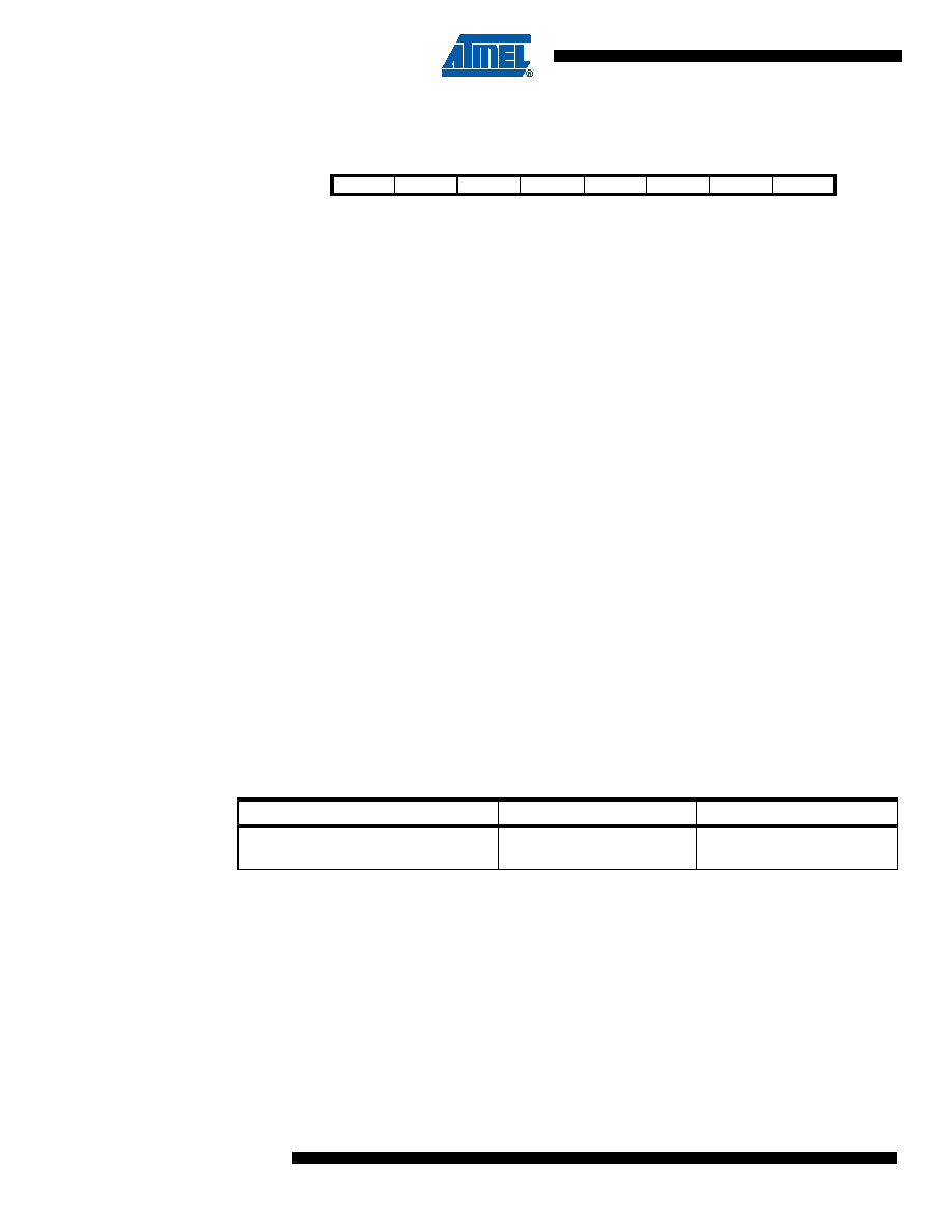
Bit
7
65
4
3210
Rd
FHB7
FHB6
FHB5
FHB4
FHB3
FHB2
FHB1
FHB0
Table 25-5.
SPM Programming Time.
Symbol
Min Programming Time
Max Programming Time
Flash write (Page Erase, Page Write,
and write Lock bits by SPM)
3.7 ms
4.5 ms
相关PDF资料 |
PDF描述 |
|---|---|
| ADG1434YRUZ | IC SWITCH QUAD SPDT 20TSSOP |
| DSPIC33FJ12MC202T-I/SS | IC DSPIC MCU/DSP 12K 28SSOP |
| PIC18F67J10T-I/PT | IC PIC MCU FLASH 64KX16 64TQFP |
| ADG509FBRNZ | IC MULTIPLEXER DUAL 4X1 16SOIC |
| PIC16C770T-I/SS | IC MCU OTP 2KX14 A/D PWM 20SSOP |
相关代理商/技术参数 |
参数描述 |
|---|---|
| PIC16HV540/JW | 功能描述:8位微控制器 -MCU .75KB 25 RAM 12 I/O RoHS:否 制造商:Silicon Labs 核心:8051 处理器系列:C8051F39x 数据总线宽度:8 bit 最大时钟频率:50 MHz 程序存储器大小:16 KB 数据 RAM 大小:1 KB 片上 ADC:Yes 工作电源电压:1.8 V to 3.6 V 工作温度范围:- 40 C to + 105 C 封装 / 箱体:QFN-20 安装风格:SMD/SMT |
| PIC16HV540-04/P | 功能描述:8位微控制器 -MCU .75KB 25 RAM 12 I/O 4MHz PDIP18 RoHS:否 制造商:Silicon Labs 核心:8051 处理器系列:C8051F39x 数据总线宽度:8 bit 最大时钟频率:50 MHz 程序存储器大小:16 KB 数据 RAM 大小:1 KB 片上 ADC:Yes 工作电源电压:1.8 V to 3.6 V 工作温度范围:- 40 C to + 105 C 封装 / 箱体:QFN-20 安装风格:SMD/SMT |
| PIC16HV540-04/P | 制造商:Microchip Technology Inc 功能描述:IC 8BIT CMOS MCU 16HV540 DIP18 |
| PIC16HV540-04/SO | 功能描述:8位微控制器 -MCU .75KB 25 RAM 12 I/O 4MHz SOIC18 RoHS:否 制造商:Silicon Labs 核心:8051 处理器系列:C8051F39x 数据总线宽度:8 bit 最大时钟频率:50 MHz 程序存储器大小:16 KB 数据 RAM 大小:1 KB 片上 ADC:Yes 工作电源电压:1.8 V to 3.6 V 工作温度范围:- 40 C to + 105 C 封装 / 箱体:QFN-20 安装风格:SMD/SMT |
| PIC16HV540-04/SS | 功能描述:8位微控制器 -MCU .75KB 25 RAM 12 I/O 4MHz SSOP20 RoHS:否 制造商:Silicon Labs 核心:8051 处理器系列:C8051F39x 数据总线宽度:8 bit 最大时钟频率:50 MHz 程序存储器大小:16 KB 数据 RAM 大小:1 KB 片上 ADC:Yes 工作电源电压:1.8 V to 3.6 V 工作温度范围:- 40 C to + 105 C 封装 / 箱体:QFN-20 安装风格:SMD/SMT |
发布紧急采购,3分钟左右您将得到回复。