- 您现在的位置:买卖IC网 > PDF目录11472 > PIC16LC62B-04/SO (Microchip Technology)IC MCU OTP 2KX14 PWM 28SOIC PDF资料下载
参数资料
| 型号: | PIC16LC62B-04/SO |
| 厂商: | Microchip Technology |
| 文件页数: | 57/120页 |
| 文件大小: | 0K |
| 描述: | IC MCU OTP 2KX14 PWM 28SOIC |
| 产品培训模块: | Asynchronous Stimulus |
| 标准包装: | 27 |
| 系列: | PIC® 16C |
| 核心处理器: | PIC |
| 芯体尺寸: | 8-位 |
| 速度: | 4MHz |
| 连通性: | I²C,SPI |
| 外围设备: | 欠压检测/复位,POR,PWM,WDT |
| 输入/输出数: | 22 |
| 程序存储器容量: | 3.5KB(2K x 14) |
| 程序存储器类型: | OTP |
| RAM 容量: | 128 x 8 |
| 电压 - 电源 (Vcc/Vdd): | 2.5 V ~ 5.5 V |
| 振荡器型: | 外部 |
| 工作温度: | 0°C ~ 70°C |
| 封装/外壳: | 28-SOIC(0.295",7.50mm 宽) |
| 包装: | 管件 |
第1页第2页第3页第4页第5页第6页第7页第8页第9页第10页第11页第12页第13页第14页第15页第16页第17页第18页第19页第20页第21页第22页第23页第24页第25页第26页第27页第28页第29页第30页第31页第32页第33页第34页第35页第36页第37页第38页第39页第40页第41页第42页第43页第44页第45页第46页第47页第48页第49页第50页第51页第52页第53页第54页第55页第56页当前第57页第58页第59页第60页第61页第62页第63页第64页第65页第66页第67页第68页第69页第70页第71页第72页第73页第74页第75页第76页第77页第78页第79页第80页第81页第82页第83页第84页第85页第86页第87页第88页第89页第90页第91页第92页第93页第94页第95页第96页第97页第98页第99页第100页第101页第102页第103页第104页第105页第106页第107页第108页第109页第110页第111页第112页第113页第114页第115页第116页第117页第118页第119页第120页
PIC16C62B/72A
1999 Microchip Technology Inc.
Preliminary
DS35008B-page 41
8.3
SSP I2C Operation
The SSP module in I2C mode fully implements all slave
functions, except general call support, and provides
interrupts on start and stop bits in hardware to support
firmware implementations of the master functions. The
SSP module implements the standard mode specifica-
tions, as well as 7-bit and 10-bit addressing.
Two pins are used for data transfer. These are the
RC3/SCK/SCL pin, which is the clock (SCL), and the
RC4/SDI/SDA pin, which is the data (SDA). The user
must configure these pins as inputs or outputs through
the TRISC<4:3> bits.
The SSP module functions are enabled by setting SSP
Enable bit SSPEN (SSPCON<5>).
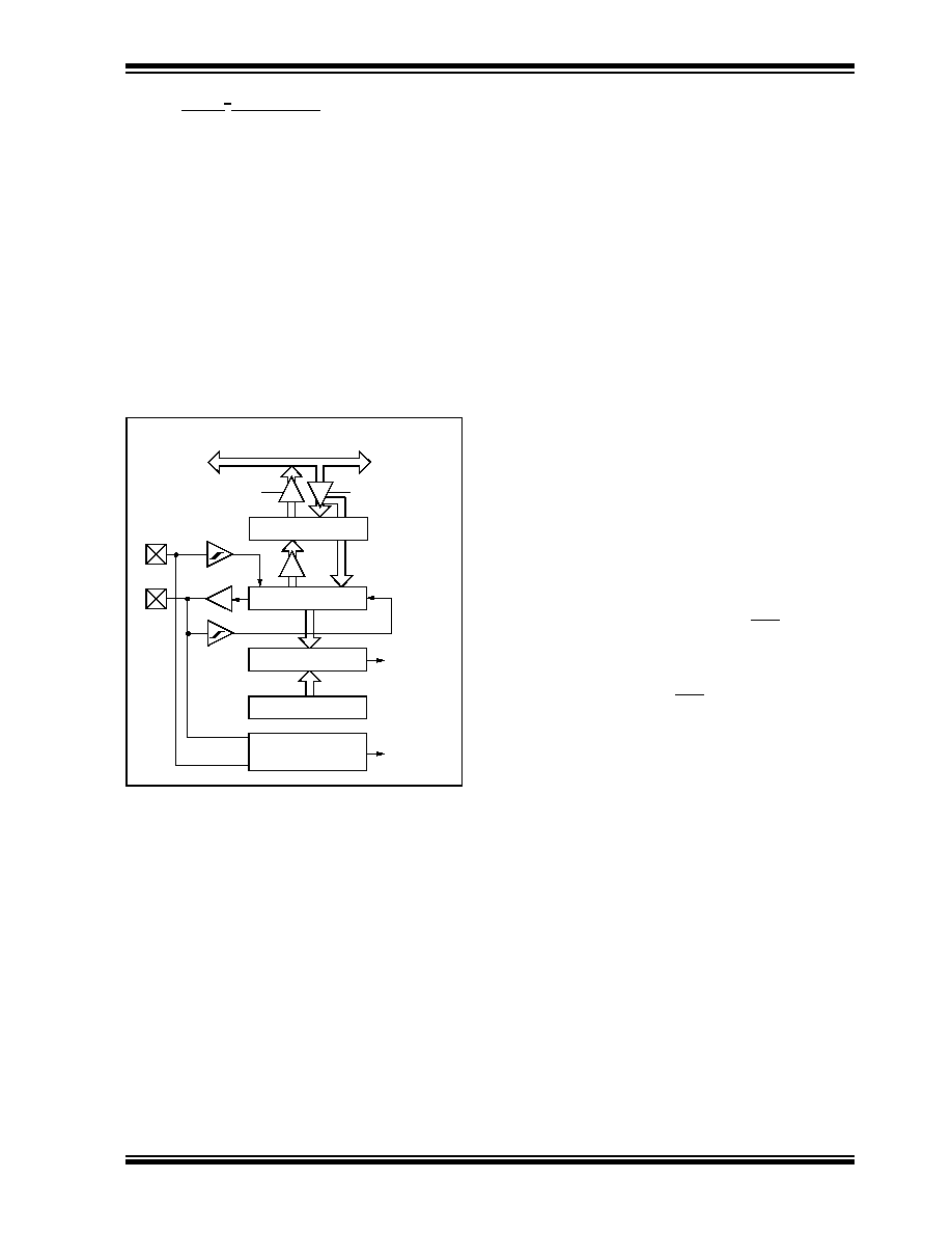
FIGURE 8-2:
SSP BLOCK DIAGRAM
(I2C MODE)
The SSP module has five registers for I2C operation.
These are the:
SSP Control Register (SSPCON)
SSP Status Register (SSPSTAT)
Serial Receive/Transmit Buffer (SSPBUF)
SSP Shift Register (SSPSR) - Not accessible
SSP Address Register (SSPADD)
The SSPCON register allows control of the I2C opera-
tion. Four mode selection bits (SSPCON<3:0>) allow
one of the following I2C modes to be selected:
I2C Slave mode (7-bit address)
I2C Slave mode (10-bit address)
I2C Slave mode (7-bit address), with start and
stop bit interrupts enabled for firmware master
mode support
I2C Slave mode (10-bit address), with start and
stop bit interrupts enabled for firmware master
mode support
I2C start and stop bit interrupts enabled for firm-
ware master mode support, slave mode idle
Selection of any I2C mode, with the SSPEN bit set,
forces the SCL and SDA pins to be operated as open
drain outputs, provided these pins are programmed to
inputs by setting the appropriate TRISC bits.
Additional information on SSP I2C operation may be
found in the PICmicro Mid-Range Reference Manual,
(DS33023).
8.3.1
SLAVE MODE
In slave mode, the SCL and SDA pins must be config-
ured as inputs (TRISC<4:3> set). The SSP module will
override the input state with the output data when
required (slave-transmitter).
When an address is matched or the data transfer after
an address match is received, the hardware automati-
cally will generate the acknowledge (ACK) pulse, and
load the SSPBUF register with the received value in the
SSPSR register.
There are certain conditions that will cause the SSP
module not to give this ACK pulse. This happens if
either of the following conditions occur:
a)
The buffer full bit BF (SSPSTAT<0>) was set
before the transfer was completed.
b)
The overflow bit SSPOV (SSPCON<6>) was set
before the transfer was completed.
In this case, the SSPSR register value is not loaded
into the SSPBUF, but bit SSPIF (PIR1<3>) is set.
Table 8-2 shows what happens when a data transfer
byte is received, given the status of bits BF and SSPOV.
The shaded cells show the condition where user soft-
ware did not properly clear the overflow condition. Flag
bit BF is cleared by reading the SSPBUF register, while
bit SSPOV is cleared through software.
The SCL clock input must have a minimum high and
low for proper operation. The high and low times of the
I2C specification, as well as the requirement of the SSP
module, is shown in timing parameter #100, THIGH, and
parameter #101, TLOW.
Read
Write
SSPSR reg
Match detect
SSPADD reg
Start and
Stop bit detect
SSPBUF reg
Internal
Data Bus
Addr Match
Set, Reset
S, P bits
(SSPSTAT reg)
RC3/SCK/SCL
RC4/
shift
clock
MSb
SDI/
LSb
SDA
相关PDF资料 |
PDF描述 |
|---|---|
| VI-B21-IX-S | CONVERTER MOD DC/DC 12V 75W |
| VI-B6V-CU-F4 | CONVERTER MOD DC/DC 5.8V 200W |
| PIC16LC62B-04/SP | IC MCU OTP 2KX14 PWM 28DIP |
| VI-B21-IW-S | CONVERTER MOD DC/DC 12V 100W |
| VI-B6V-CU-F3 | CONVERTER MOD DC/DC 5.8V 200W |
相关代理商/技术参数 |
参数描述 |
|---|---|
| PIC16LC62BT-04/SO | 功能描述:8位微控制器 -MCU 3.5KB 128 RAM 22 I/O RoHS:否 制造商:Silicon Labs 核心:8051 处理器系列:C8051F39x 数据总线宽度:8 bit 最大时钟频率:50 MHz 程序存储器大小:16 KB 数据 RAM 大小:1 KB 片上 ADC:Yes 工作电源电压:1.8 V to 3.6 V 工作温度范围:- 40 C to + 105 C 封装 / 箱体:QFN-20 安装风格:SMD/SMT |
| PIC16LC62BT-04/SS | 功能描述:8位微控制器 -MCU 3.5KB 128 RAM 22 I/O RoHS:否 制造商:Silicon Labs 核心:8051 处理器系列:C8051F39x 数据总线宽度:8 bit 最大时钟频率:50 MHz 程序存储器大小:16 KB 数据 RAM 大小:1 KB 片上 ADC:Yes 工作电源电压:1.8 V to 3.6 V 工作温度范围:- 40 C to + 105 C 封装 / 箱体:QFN-20 安装风格:SMD/SMT |
| PIC16LC62BT-04I/ML | 功能描述:8位微控制器 -MCU 3.5KB 128 RAM 22 I/O RoHS:否 制造商:Silicon Labs 核心:8051 处理器系列:C8051F39x 数据总线宽度:8 bit 最大时钟频率:50 MHz 程序存储器大小:16 KB 数据 RAM 大小:1 KB 片上 ADC:Yes 工作电源电压:1.8 V to 3.6 V 工作温度范围:- 40 C to + 105 C 封装 / 箱体:QFN-20 安装风格:SMD/SMT |
| PIC16LC62BT-04I/SO | 功能描述:8位微控制器 -MCU 3.5KB 128 RAM 22 I/O RoHS:否 制造商:Silicon Labs 核心:8051 处理器系列:C8051F39x 数据总线宽度:8 bit 最大时钟频率:50 MHz 程序存储器大小:16 KB 数据 RAM 大小:1 KB 片上 ADC:Yes 工作电源电压:1.8 V to 3.6 V 工作温度范围:- 40 C to + 105 C 封装 / 箱体:QFN-20 安装风格:SMD/SMT |
| PIC16LC62BT-04I/SS | 功能描述:8位微控制器 -MCU 3.5KB 128 RAM 22 I/O RoHS:否 制造商:Silicon Labs 核心:8051 处理器系列:C8051F39x 数据总线宽度:8 bit 最大时钟频率:50 MHz 程序存储器大小:16 KB 数据 RAM 大小:1 KB 片上 ADC:Yes 工作电源电压:1.8 V to 3.6 V 工作温度范围:- 40 C to + 105 C 封装 / 箱体:QFN-20 安装风格:SMD/SMT |
发布紧急采购,3分钟左右您将得到回复。