- 您现在的位置:买卖IC网 > PDF目录11472 > PIC16LC62B-04/SO (Microchip Technology)IC MCU OTP 2KX14 PWM 28SOIC PDF资料下载
参数资料
| 型号: | PIC16LC62B-04/SO |
| 厂商: | Microchip Technology |
| 文件页数: | 85/120页 |
| 文件大小: | 0K |
| 描述: | IC MCU OTP 2KX14 PWM 28SOIC |
| 产品培训模块: | Asynchronous Stimulus |
| 标准包装: | 27 |
| 系列: | PIC® 16C |
| 核心处理器: | PIC |
| 芯体尺寸: | 8-位 |
| 速度: | 4MHz |
| 连通性: | I²C,SPI |
| 外围设备: | 欠压检测/复位,POR,PWM,WDT |
| 输入/输出数: | 22 |
| 程序存储器容量: | 3.5KB(2K x 14) |
| 程序存储器类型: | OTP |
| RAM 容量: | 128 x 8 |
| 电压 - 电源 (Vcc/Vdd): | 2.5 V ~ 5.5 V |
| 振荡器型: | 外部 |
| 工作温度: | 0°C ~ 70°C |
| 封装/外壳: | 28-SOIC(0.295",7.50mm 宽) |
| 包装: | 管件 |
第1页第2页第3页第4页第5页第6页第7页第8页第9页第10页第11页第12页第13页第14页第15页第16页第17页第18页第19页第20页第21页第22页第23页第24页第25页第26页第27页第28页第29页第30页第31页第32页第33页第34页第35页第36页第37页第38页第39页第40页第41页第42页第43页第44页第45页第46页第47页第48页第49页第50页第51页第52页第53页第54页第55页第56页第57页第58页第59页第60页第61页第62页第63页第64页第65页第66页第67页第68页第69页第70页第71页第72页第73页第74页第75页第76页第77页第78页第79页第80页第81页第82页第83页第84页当前第85页第86页第87页第88页第89页第90页第91页第92页第93页第94页第95页第96页第97页第98页第99页第100页第101页第102页第103页第104页第105页第106页第107页第108页第109页第110页第111页第112页第113页第114页第115页第116页第117页第118页第119页第120页
PIC16C62B/72A
1999 Microchip Technology Inc.
Preliminary
DS35008B-page 67
11.0
INSTRUCTION SET SUMMARY
Each PIC16CXXX instruction is a 14-bit word divided
into an OPCODE which specifies the instruction type
and one or more operands which further specify the
operation of the instruction. The PIC16CXX instruction
set summary in Table 11-2 lists byte-oriented, bit-ori-
ented, and literal and control operations. Table 11-1
shows the opcode field descriptions.
For byte-oriented instructions, ’f’ represents a file reg-
ister designator and ’d’ represents a destination desig-
nator. The file register designator specifies which file
register is to be used by the instruction.
The destination designator specifies where the result of
the operation is to be placed. If ’d’ is zero, the result is
placed in the W register. If ’d’ is one, the result is placed
in the file register specified in the instruction.
For bit-oriented instructions, ’b’ represents a bit field
designator which selects the number of the bit affected
by the operation, while ’f’ represents the number of the
file in which the bit is located.
For literal and control operations, ’k’ represents an
eight or eleven bit constant or literal value.
TABLE 11-1
OPCODE FIELD
DESCRIPTIONS
The instruction set is highly orthogonal and is grouped
into three basic categories:
Byte-oriented operations
Bit-oriented operations
Literal and control operations
All instructions are executed within one single instruc-
tion cycle, unless a conditional test is true or the pro-
gram counter is changed as a result of an instruction.
In this case, the execution takes two instruction cycles
with the second cycle executed as a NOP. One instruc-
tion cycle consists of four oscillator periods. Thus, for
an oscillator frequency of 4 MHz, the normal instruction
execution time is 1
s. If a conditional test is true or the
program counter is changed as a result of an instruc-
tion, the instruction execution time is 2
s.
Table 11-2 lists the instructions recognized by the
MPASM assembler.
Figure 11-1 shows the general formats that the instruc-
tions can have.
All examples use the following format to represent a
hexadecimal number:
0xhh
where h signifies a hexadecimal digit.
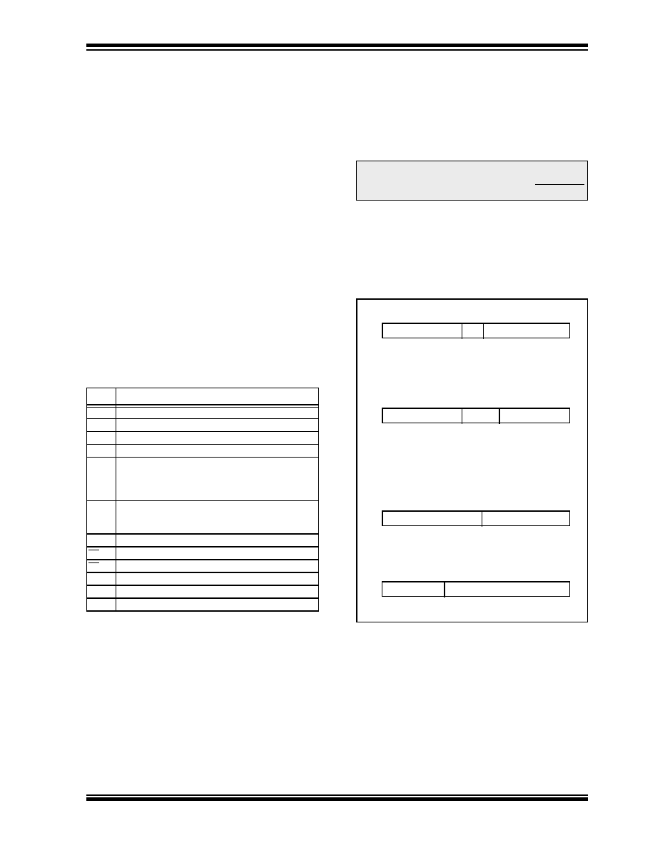
FIGURE 11-1: GENERAL FORMAT FOR
INSTRUCTIONS
A description of each instruction is available in the
PICmicro
Mid-Range
Reference
Manual,
(DS33023).
Field
Description
f
Register file address (0x00 to 0x7F)
W
Working register (accumulator)
b
Bit address within an 8-bit file register
k
Literal field, constant data or label
x
Don’t care location (= 0 or 1)
The assembler will generate code with x = 0. It is the
recommended form of use for compatibility with all
Microchip software tools.
d
Destination select; d = 0: store result in W,
d = 1: store result in file register f.
Default is d = 1
PC
Program Counter
TO
Time-out bit
PD
Power-down bit
Z
Zero bit
DC
Digit Carry bit
C
Carry bit
Note:
To maintain upward compatibility with
future PIC16CXXX products, do not use
the OPTION and TRIS instructions.
Byte-oriented file register operations
13
8
7
6
0
d = 0 for destination W
OPCODE
d
f (FILE #)
d = 1 for destination f
f = 7-bit file register address
Bit-oriented file register operations
13
10 9
7 6
0
OPCODE
b (BIT #)
f (FILE #)
b = 3-bit bit address
f = 7-bit file register address
Literal and control operations
13
8
7
0
OPCODE
k (literal)
k = 8-bit immediate value
13
11
10
0
OPCODE
k (literal)
k = 11-bit immediate value
General
CALL
and GOTO instructions only
相关PDF资料 |
PDF描述 |
|---|---|
| VI-B21-IX-S | CONVERTER MOD DC/DC 12V 75W |
| VI-B6V-CU-F4 | CONVERTER MOD DC/DC 5.8V 200W |
| PIC16LC62B-04/SP | IC MCU OTP 2KX14 PWM 28DIP |
| VI-B21-IW-S | CONVERTER MOD DC/DC 12V 100W |
| VI-B6V-CU-F3 | CONVERTER MOD DC/DC 5.8V 200W |
相关代理商/技术参数 |
参数描述 |
|---|---|
| PIC16LC62BT-04/SO | 功能描述:8位微控制器 -MCU 3.5KB 128 RAM 22 I/O RoHS:否 制造商:Silicon Labs 核心:8051 处理器系列:C8051F39x 数据总线宽度:8 bit 最大时钟频率:50 MHz 程序存储器大小:16 KB 数据 RAM 大小:1 KB 片上 ADC:Yes 工作电源电压:1.8 V to 3.6 V 工作温度范围:- 40 C to + 105 C 封装 / 箱体:QFN-20 安装风格:SMD/SMT |
| PIC16LC62BT-04/SS | 功能描述:8位微控制器 -MCU 3.5KB 128 RAM 22 I/O RoHS:否 制造商:Silicon Labs 核心:8051 处理器系列:C8051F39x 数据总线宽度:8 bit 最大时钟频率:50 MHz 程序存储器大小:16 KB 数据 RAM 大小:1 KB 片上 ADC:Yes 工作电源电压:1.8 V to 3.6 V 工作温度范围:- 40 C to + 105 C 封装 / 箱体:QFN-20 安装风格:SMD/SMT |
| PIC16LC62BT-04I/ML | 功能描述:8位微控制器 -MCU 3.5KB 128 RAM 22 I/O RoHS:否 制造商:Silicon Labs 核心:8051 处理器系列:C8051F39x 数据总线宽度:8 bit 最大时钟频率:50 MHz 程序存储器大小:16 KB 数据 RAM 大小:1 KB 片上 ADC:Yes 工作电源电压:1.8 V to 3.6 V 工作温度范围:- 40 C to + 105 C 封装 / 箱体:QFN-20 安装风格:SMD/SMT |
| PIC16LC62BT-04I/SO | 功能描述:8位微控制器 -MCU 3.5KB 128 RAM 22 I/O RoHS:否 制造商:Silicon Labs 核心:8051 处理器系列:C8051F39x 数据总线宽度:8 bit 最大时钟频率:50 MHz 程序存储器大小:16 KB 数据 RAM 大小:1 KB 片上 ADC:Yes 工作电源电压:1.8 V to 3.6 V 工作温度范围:- 40 C to + 105 C 封装 / 箱体:QFN-20 安装风格:SMD/SMT |
| PIC16LC62BT-04I/SS | 功能描述:8位微控制器 -MCU 3.5KB 128 RAM 22 I/O RoHS:否 制造商:Silicon Labs 核心:8051 处理器系列:C8051F39x 数据总线宽度:8 bit 最大时钟频率:50 MHz 程序存储器大小:16 KB 数据 RAM 大小:1 KB 片上 ADC:Yes 工作电源电压:1.8 V to 3.6 V 工作温度范围:- 40 C to + 105 C 封装 / 箱体:QFN-20 安装风格:SMD/SMT |
发布紧急采购,3分钟左右您将得到回复。