- 您现在的位置:买卖IC网 > PDF目录10908 > PIC16LC72-04/SO (Microchip Technology)IC MCU OTP 2KX14 A/D PWM 28SOIC PDF资料下载
参数资料
| 型号: | PIC16LC72-04/SO |
| 厂商: | Microchip Technology |
| 文件页数: | 104/111页 |
| 文件大小: | 0K |
| 描述: | IC MCU OTP 2KX14 A/D PWM 28SOIC |
| 产品培训模块: | Asynchronous Stimulus |
| 标准包装: | 27 |
| 系列: | PIC® 16C |
| 核心处理器: | PIC |
| 芯体尺寸: | 8-位 |
| 速度: | 4MHz |
| 连通性: | I²C,SPI |
| 外围设备: | 欠压检测/复位,POR,PWM,WDT |
| 输入/输出数: | 22 |
| 程序存储器容量: | 3.5KB(2K x 14) |
| 程序存储器类型: | OTP |
| RAM 容量: | 128 x 8 |
| 电压 - 电源 (Vcc/Vdd): | 2.5 V ~ 6 V |
| 数据转换器: | A/D 5x8b |
| 振荡器型: | 外部 |
| 工作温度: | 0°C ~ 70°C |
| 封装/外壳: | 28-SOIC(0.295",7.50mm 宽) |
| 包装: | 管件 |
第1页第2页第3页第4页第5页第6页第7页第8页第9页第10页第11页第12页第13页第14页第15页第16页第17页第18页第19页第20页第21页第22页第23页第24页第25页第26页第27页第28页第29页第30页第31页第32页第33页第34页第35页第36页第37页第38页第39页第40页第41页第42页第43页第44页第45页第46页第47页第48页第49页第50页第51页第52页第53页第54页第55页第56页第57页第58页第59页第60页第61页第62页第63页第64页第65页第66页第67页第68页第69页第70页第71页第72页第73页第74页第75页第76页第77页第78页第79页第80页第81页第82页第83页第84页第85页第86页第87页第88页第89页第90页第91页第92页第93页第94页第95页第96页第97页第98页第99页第100页第101页第102页第103页当前第104页第105页第106页第107页第108页第109页第110页第111页
PIC18FXX2
DS39564C-page 90
2006 Microchip Technology Inc.
9.2
PORTB, TRISB and LATB
Registers
PORTB is an 8-bit wide, bi-directional port. The corre-
sponding Data Direction register is TRISB. Setting a
TRISB bit (= 1) will make the corresponding PORTB pin
an input (i.e., put the corresponding output driver in a
Hi-Impedance mode). Clearing a TRISB bit (= 0) will
make the corresponding PORTB pin an output (i.e., put
the contents of the output latch on the selected pin).
The Data Latch register (LATB) is also memory
mapped. Read-modify-write operations on the LATB
register reads and writes the latched output value for
PORTB.
EXAMPLE 9-2:
INITIALIZING PORTB
Each of the PORTB pins has a weak internal pull-up. A
single control bit can turn on all the pull-ups. This is per-
formed by clearing bit RBPU (INTCON2<7>). The
weak pull-up is automatically turned off when the port
pin is configured as an output. The pull-ups are
disabled on a Power-on Reset.
Four of the PORTB pins, RB7:RB4, have an interrupt-
on-change feature. Only pins configured as inputs can
cause this interrupt to occur (i.e., any RB7:RB4 pin
configured as an output is excluded from the interrupt-
on-change comparison). The input pins (of RB7:RB4)
are compared with the old value latched on the last
read of PORTB. The “mismatch” outputs of RB7:RB4
are OR’ed together to generate the RB Port Change
Interrupt with flag bit, RBIF (INTCON<0>).
This interrupt can wake the device from SLEEP. The
user, in the Interrupt Service Routine, can clear the
interrupt in the following manner:
a)
Any read or write of PORTB (except with the
MOVFF
instruction). This will end the mismatch
condition.
b)
Clear flag bit RBIF.
A mismatch condition will continue to set flag bit RBIF.
Reading PORTB will end the mismatch condition and
allow flag bit RBIF to be cleared.
The interrupt-on-change feature is recommended for
wake-up on key depression operation and operations
where PORTB is only used for the interrupt-on-change
feature. Polling of PORTB is not recommended while
using the interrupt-on-change feature.
RB3 can be configured by the configuration bit
CCP2MX as the alternate peripheral pin for the CCP2
module (CCP2MX=’0’).
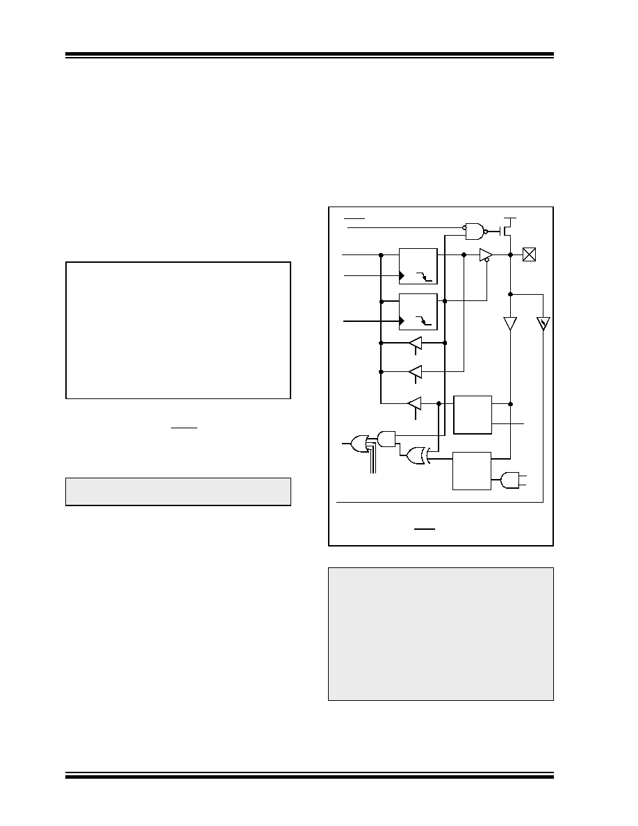
FIGURE 9-4:
BLOCK DIAGRAM OF
RB7:RB4 PINS
Note:
On a Power-on Reset, these pins are
configured as digital inputs.
CLRF
PORTB
; Initialize PORTB by
; clearing output
; data latches
CLRF
LATB
; Alternate method
; to clear output
; data latches
MOVLW 0xCF
; Value used to
; initialize data
; direction
MOVWF TRISB
; Set RB<3:0> as inputs
; RB<5:4> as outputs
; RB<7:6> as inputs
Note 1: While in Low Voltage ICSP mode, the
RB5 pin can no longer be used as a gen-
eral purpose I/O pin, and should be held
low during normal operation to protect
against inadvertent ICSP mode entry.
2: When using Low Voltage ICSP program-
ming (LVP), the pull-up on RB5 becomes
disabled. If TRISB bit 5 is cleared,
thereby setting RB5 as an output, LATB
bit 5 must also be cleared for proper
operation.
Data Latch
From other
RBPU(2)
P
VDD
I/O pin(1)
Q
D
CK
Q
D
CK
QD
EN
QD
EN
Data Bus
WR LATB
WR TRISB
Set RBIF
TRIS Latch
RD TRISB
RD PORTB
RB7:RB4 pins
Weak
Pull-up
RD PORTB
Latch
TTL
Input
Buffer
ST
Buffer
RB7:RB5 in Serial Programming mode
Q3
Q1
RD LATB
or
PORTB
Note 1:
I/O pins have diode protection to VDD and VSS.
2:
To enable weak pull-ups, set the appropriate TRIS bit(s)
and clear the RBPU bit (INTCON2<7>).
相关PDF资料 |
PDF描述 |
|---|---|
| PIC16C72-20/SS | IC MCU OTP 2KX14 A/D PWM 28SSOP |
| PIC16C72-04/SS | IC MCU OTP 2KX14 A/D PWM 28SSOP |
| PIC16C72/JW | IC MCU EPROM2KX14 A/D PWM 28CDIP |
| PIC16C711/JW | IC MCU EPROM 1KX14 A/D 18CDIP |
| SI2400-FS | IC ISOMODEM SYST-SIDE DAA 16SOIC |
相关代理商/技术参数 |
参数描述 |
|---|---|
| PIC16LC72A-04/SO | 功能描述:8位微控制器 -MCU 3.5KB 128 RAM 22 I/O RoHS:否 制造商:Silicon Labs 核心:8051 处理器系列:C8051F39x 数据总线宽度:8 bit 最大时钟频率:50 MHz 程序存储器大小:16 KB 数据 RAM 大小:1 KB 片上 ADC:Yes 工作电源电压:1.8 V to 3.6 V 工作温度范围:- 40 C to + 105 C 封装 / 箱体:QFN-20 安装风格:SMD/SMT |
| PIC16LC72A-04/SP | 功能描述:8位微控制器 -MCU 3.5KB 128 RAM 22 I/O RoHS:否 制造商:Silicon Labs 核心:8051 处理器系列:C8051F39x 数据总线宽度:8 bit 最大时钟频率:50 MHz 程序存储器大小:16 KB 数据 RAM 大小:1 KB 片上 ADC:Yes 工作电源电压:1.8 V to 3.6 V 工作温度范围:- 40 C to + 105 C 封装 / 箱体:QFN-20 安装风格:SMD/SMT |
| PIC16LC72A-04/SS | 功能描述:8位微控制器 -MCU 3.5KB 128 RAM 22 I/O RoHS:否 制造商:Silicon Labs 核心:8051 处理器系列:C8051F39x 数据总线宽度:8 bit 最大时钟频率:50 MHz 程序存储器大小:16 KB 数据 RAM 大小:1 KB 片上 ADC:Yes 工作电源电压:1.8 V to 3.6 V 工作温度范围:- 40 C to + 105 C 封装 / 箱体:QFN-20 安装风格:SMD/SMT |
| PIC16LC72A-04I/ML | 功能描述:8位微控制器 -MCU 3.5KB 128 RAM 22 I/O RoHS:否 制造商:Silicon Labs 核心:8051 处理器系列:C8051F39x 数据总线宽度:8 bit 最大时钟频率:50 MHz 程序存储器大小:16 KB 数据 RAM 大小:1 KB 片上 ADC:Yes 工作电源电压:1.8 V to 3.6 V 工作温度范围:- 40 C to + 105 C 封装 / 箱体:QFN-20 安装风格:SMD/SMT |
| PIC16LC72A-04I/SO | 功能描述:8位微控制器 -MCU 3.5KB 128 RAM 22 I/O RoHS:否 制造商:Silicon Labs 核心:8051 处理器系列:C8051F39x 数据总线宽度:8 bit 最大时钟频率:50 MHz 程序存储器大小:16 KB 数据 RAM 大小:1 KB 片上 ADC:Yes 工作电源电压:1.8 V to 3.6 V 工作温度范围:- 40 C to + 105 C 封装 / 箱体:QFN-20 安装风格:SMD/SMT |
发布紧急采购,3分钟左右您将得到回复。