- 您现在的位置:买卖IC网 > PDF目录10908 > PIC16LC72-04/SO (Microchip Technology)IC MCU OTP 2KX14 A/D PWM 28SOIC PDF资料下载
参数资料
| 型号: | PIC16LC72-04/SO |
| 厂商: | Microchip Technology |
| 文件页数: | 20/111页 |
| 文件大小: | 0K |
| 描述: | IC MCU OTP 2KX14 A/D PWM 28SOIC |
| 产品培训模块: | Asynchronous Stimulus |
| 标准包装: | 27 |
| 系列: | PIC® 16C |
| 核心处理器: | PIC |
| 芯体尺寸: | 8-位 |
| 速度: | 4MHz |
| 连通性: | I²C,SPI |
| 外围设备: | 欠压检测/复位,POR,PWM,WDT |
| 输入/输出数: | 22 |
| 程序存储器容量: | 3.5KB(2K x 14) |
| 程序存储器类型: | OTP |
| RAM 容量: | 128 x 8 |
| 电压 - 电源 (Vcc/Vdd): | 2.5 V ~ 6 V |
| 数据转换器: | A/D 5x8b |
| 振荡器型: | 外部 |
| 工作温度: | 0°C ~ 70°C |
| 封装/外壳: | 28-SOIC(0.295",7.50mm 宽) |
| 包装: | 管件 |
第1页第2页第3页第4页第5页第6页第7页第8页第9页第10页第11页第12页第13页第14页第15页第16页第17页第18页第19页当前第20页第21页第22页第23页第24页第25页第26页第27页第28页第29页第30页第31页第32页第33页第34页第35页第36页第37页第38页第39页第40页第41页第42页第43页第44页第45页第46页第47页第48页第49页第50页第51页第52页第53页第54页第55页第56页第57页第58页第59页第60页第61页第62页第63页第64页第65页第66页第67页第68页第69页第70页第71页第72页第73页第74页第75页第76页第77页第78页第79页第80页第81页第82页第83页第84页第85页第86页第87页第88页第89页第90页第91页第92页第93页第94页第95页第96页第97页第98页第99页第100页第101页第102页第103页第104页第105页第106页第107页第108页第109页第110页第111页
PIC16C72 Series
DS39016A-page 16
Preliminary
1998 Microchip Technology Inc.
2.3.1
STACK
The stack allows a combination of up to 8 program calls
and interrupts to occur. The stack contains the return
address from this branch in program execution.
Midrange devices have an 8 level deep x 13-bit wide
hardware stack. The stack space is not part of either
program or data space and the stack pointer is not
readable or writable. The PC is PUSHed onto the stack
when a CALL instruction is executed or an interrupt
causes a branch. The stack is POPed in the event of a
RETURN,
RETLW
or a RETFIE instruction execution.
PCLATH is not modied when the stack is PUSHed or
POPed.
After the stack has been PUSHed eight times, the ninth
push overwrites the value that was stored from the rst
push. The tenth push overwrites the second push (and
so on). An example of the overwriting of the stack is
shown in Figure 2-10.
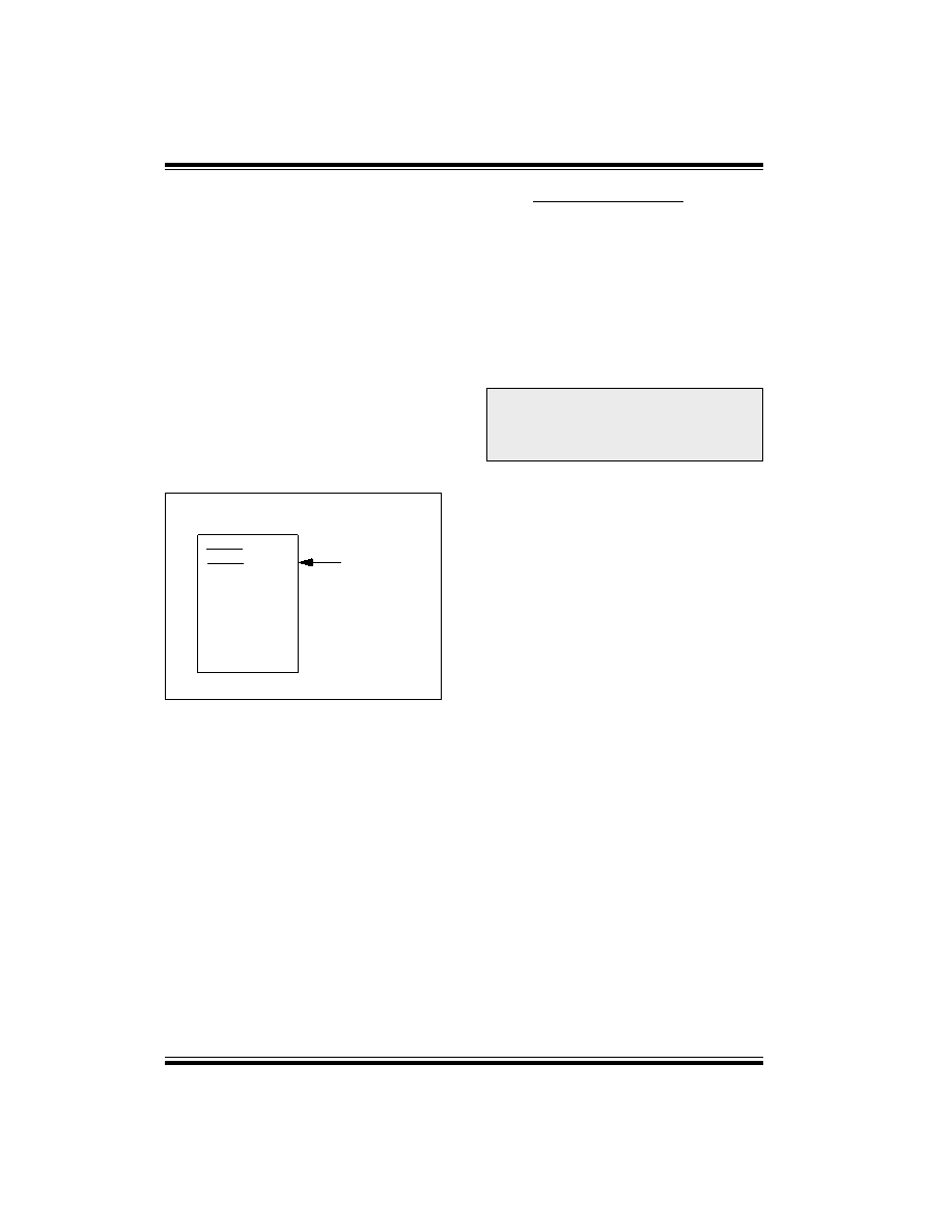
FIGURE 2-10: STACK MODIFICATION
2.4
Program Memory Paging
The CALL and GOTO instructions provide 11 bits of
address to allow branching within any 2K program
memory page. When doing a CALL or GOTO instruction
the upper 2 bits of the address are provided by
PCLATH<4:3>. When doing a CALL or GOTO instruction,
the user must ensure that the page select bits are pro-
grammed so that the desired program memory page is
addressed. If a return from a CALL instruction (or inter-
rupt) is executed, the entire 13-bit PC is pushed onto
the
stack.
Therefore,
manipulation
of
the
PCLATH<4:3> bits are not required for the return
instructions (which POPs the address from the stack).
Push1 Push9
Push2 Push10
Push3
Push4
Push5
Push6
Push7
Push8
Top of STACK
STACK
Note:
PIC16C72 Series devices ignore paging
bit PCLATH<4>. The use of PCLATH<4>
as a general purpose read/write bit is not
recommended
since
this
may
affect
upward compatibility with future products.
相关PDF资料 |
PDF描述 |
|---|---|
| PIC16C72-20/SS | IC MCU OTP 2KX14 A/D PWM 28SSOP |
| PIC16C72-04/SS | IC MCU OTP 2KX14 A/D PWM 28SSOP |
| PIC16C72/JW | IC MCU EPROM2KX14 A/D PWM 28CDIP |
| PIC16C711/JW | IC MCU EPROM 1KX14 A/D 18CDIP |
| SI2400-FS | IC ISOMODEM SYST-SIDE DAA 16SOIC |
相关代理商/技术参数 |
参数描述 |
|---|---|
| PIC16LC72A-04/SO | 功能描述:8位微控制器 -MCU 3.5KB 128 RAM 22 I/O RoHS:否 制造商:Silicon Labs 核心:8051 处理器系列:C8051F39x 数据总线宽度:8 bit 最大时钟频率:50 MHz 程序存储器大小:16 KB 数据 RAM 大小:1 KB 片上 ADC:Yes 工作电源电压:1.8 V to 3.6 V 工作温度范围:- 40 C to + 105 C 封装 / 箱体:QFN-20 安装风格:SMD/SMT |
| PIC16LC72A-04/SP | 功能描述:8位微控制器 -MCU 3.5KB 128 RAM 22 I/O RoHS:否 制造商:Silicon Labs 核心:8051 处理器系列:C8051F39x 数据总线宽度:8 bit 最大时钟频率:50 MHz 程序存储器大小:16 KB 数据 RAM 大小:1 KB 片上 ADC:Yes 工作电源电压:1.8 V to 3.6 V 工作温度范围:- 40 C to + 105 C 封装 / 箱体:QFN-20 安装风格:SMD/SMT |
| PIC16LC72A-04/SS | 功能描述:8位微控制器 -MCU 3.5KB 128 RAM 22 I/O RoHS:否 制造商:Silicon Labs 核心:8051 处理器系列:C8051F39x 数据总线宽度:8 bit 最大时钟频率:50 MHz 程序存储器大小:16 KB 数据 RAM 大小:1 KB 片上 ADC:Yes 工作电源电压:1.8 V to 3.6 V 工作温度范围:- 40 C to + 105 C 封装 / 箱体:QFN-20 安装风格:SMD/SMT |
| PIC16LC72A-04I/ML | 功能描述:8位微控制器 -MCU 3.5KB 128 RAM 22 I/O RoHS:否 制造商:Silicon Labs 核心:8051 处理器系列:C8051F39x 数据总线宽度:8 bit 最大时钟频率:50 MHz 程序存储器大小:16 KB 数据 RAM 大小:1 KB 片上 ADC:Yes 工作电源电压:1.8 V to 3.6 V 工作温度范围:- 40 C to + 105 C 封装 / 箱体:QFN-20 安装风格:SMD/SMT |
| PIC16LC72A-04I/SO | 功能描述:8位微控制器 -MCU 3.5KB 128 RAM 22 I/O RoHS:否 制造商:Silicon Labs 核心:8051 处理器系列:C8051F39x 数据总线宽度:8 bit 最大时钟频率:50 MHz 程序存储器大小:16 KB 数据 RAM 大小:1 KB 片上 ADC:Yes 工作电源电压:1.8 V to 3.6 V 工作温度范围:- 40 C to + 105 C 封装 / 箱体:QFN-20 安装风格:SMD/SMT |
发布紧急采购,3分钟左右您将得到回复。