- 您现在的位置:买卖IC网 > PDF目录11430 > PIC16LC781-I/SS (Microchip Technology)IC MCU OTP 1KX14 W/AD COMP20SSOP PDF资料下载
参数资料
| 型号: | PIC16LC781-I/SS |
| 厂商: | Microchip Technology |
| 文件页数: | 136/186页 |
| 文件大小: | 0K |
| 描述: | IC MCU OTP 1KX14 W/AD COMP20SSOP |
| 产品培训模块: | Asynchronous Stimulus |
| 标准包装: | 67 |
| 系列: | PIC® 16C |
| 核心处理器: | PIC |
| 芯体尺寸: | 8-位 |
| 速度: | 20MHz |
| 外围设备: | 欠压检测/复位,POR,PWM,WDT |
| 输入/输出数: | 13 |
| 程序存储器容量: | 1.75KB(1K x 14) |
| 程序存储器类型: | OTP |
| RAM 容量: | 128 x 8 |
| 电压 - 电源 (Vcc/Vdd): | 2.7 V ~ 5.5 V |
| 数据转换器: | A/D 8x8b; D/A 1x8b |
| 振荡器型: | 内部 |
| 工作温度: | -40°C ~ 85°C |
| 封装/外壳: | 20-SSOP(0.209",5.30mm 宽) |
| 包装: | 管件 |
| 其它名称: | PIC16LC781I/SS |
第1页第2页第3页第4页第5页第6页第7页第8页第9页第10页第11页第12页第13页第14页第15页第16页第17页第18页第19页第20页第21页第22页第23页第24页第25页第26页第27页第28页第29页第30页第31页第32页第33页第34页第35页第36页第37页第38页第39页第40页第41页第42页第43页第44页第45页第46页第47页第48页第49页第50页第51页第52页第53页第54页第55页第56页第57页第58页第59页第60页第61页第62页第63页第64页第65页第66页第67页第68页第69页第70页第71页第72页第73页第74页第75页第76页第77页第78页第79页第80页第81页第82页第83页第84页第85页第86页第87页第88页第89页第90页第91页第92页第93页第94页第95页第96页第97页第98页第99页第100页第101页第102页第103页第104页第105页第106页第107页第108页第109页第110页第111页第112页第113页第114页第115页第116页第117页第118页第119页第120页第121页第122页第123页第124页第125页第126页第127页第128页第129页第130页第131页第132页第133页第134页第135页当前第136页第137页第138页第139页第140页第141页第142页第143页第144页第145页第146页第147页第148页第149页第150页第151页第152页第153页第154页第155页第156页第157页第158页第159页第160页第161页第162页第163页第164页第165页第166页第167页第168页第169页第170页第171页第172页第173页第174页第175页第176页第177页第178页第179页第180页第181页第182页第183页第184页第185页第186页
2001 Microchip Technology Inc.
Preliminary
DS41171A-page 51
PIC16C781/782
5.0
TIMER0 MODULE
The Timer0 module timer/counter has the following
features:
8-bit timer/counter
Readable and writable
Internal or external clock select
Edge select for external clock
8-bit software programmable prescaler
Interrupt on overflow from FFh to 00h
Figure 5-1 is a simplified block diagram of the Timer0
module.
Additional information on timer modules is available in
the
PICmicro
Mid-Range
Reference
Manual,
(DS33023).
5.1
Timer0 Operation
Timer0 can operate as either a timer or a counter.
Programming Timer0 is via the OPTION register (see
Timer0 mode is selected by clearing/setting the bit
T0CS (OPTION_REG<5>). In Timer mode (T0CS = 0),
the Timer0 module increments every instruction cycle
(without prescaler). If the TMR0 register is written, the
increment is inhibited for the following two instruction
cycles. The user can work around this by writing an
adjusted value to the TMR0 register.
Counter mode is selected by setting bit T0CS
(OPTION_REG<5>).
In
Counter
mode,
Timer0
increments either on every rising, or falling edge of pin
RA4/T0CKI. The incrementing edge is determined by
the
Timer0
Source
Edge
Select
bit
T0SE
(OPTION_REG<4>). Clearing bit T0SE selects the ris-
ing edge, setting selects the falling edge. Restrictions
on the external clock input are discussed below.
When an external clock input is used for Timer0, it must
meet certain requirements. The requirements ensure
the external clock can be synchronized with the internal
system clock. Also, there is a delay in the actual incre-
menting of Timer0 after synchronization.
Additional information on external clock requirements
is available in the PICmicro Mid-Range Reference
Manual, (DS33023).
EXAMPLE 5-1:
INITIALIZING TIMER0
;* This code block will configure Timer0
;* for Polling, internal clock & 1:16
;*
prescaler
;*
;* Wait for TMR0 overflow code included
BANKSEL
TMR0
; Select Bank 0
CLRF
TMR0
; Clear Timer0
; Register
BANKSEL
OPTION_REG
; Select Bank 1
MOVLW
B’11000011’
; INT on L2H
MOVWF
OPTION_REG
; Internal clk,
; pscaler 1:16
********************************************
;*
Wait for TMR0 overflow
;*
T0_OVFL_WAIT
TBFSS
INTCON,T0IF
; Check for TMR0
; overflow
GOTO
T0_OVFL_WAIT
; If clear, test
; again
BCF
INTCON,T0IF
; Clear interrupt
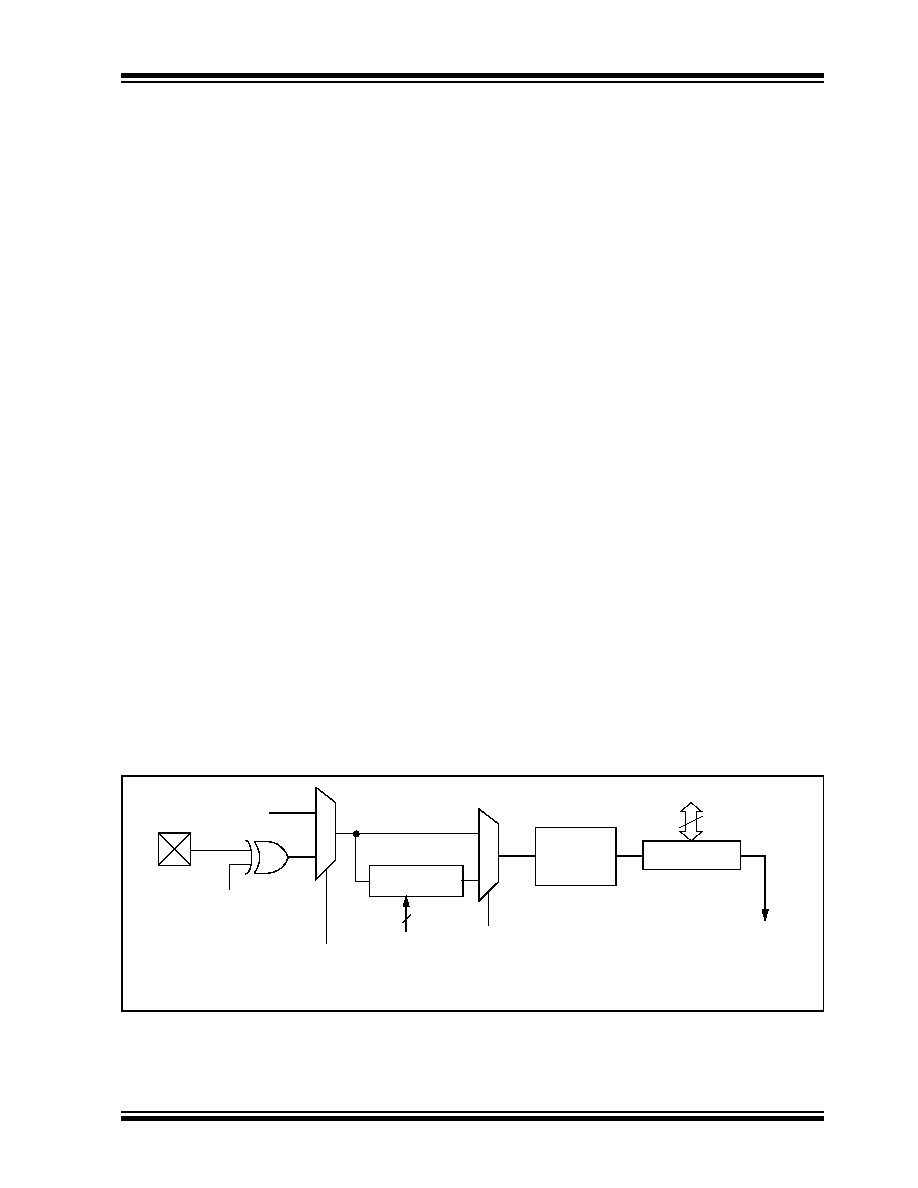
FIGURE 5-1:
TIMER0 BLOCK DIAGRAM
Note
1:
T0CS, T0SE, PSA, PS<2:0> (OPTION_REG<5:0>).
2: The prescaler is shared with Watchdog Timer (refer to Figure 5-2 for detailed block diagram).
RA4/T0CKI
T0SE
0
1
0
pin
T0CS
FOSC/4
Programmable
Prescaler
Sync with
Internal
Clocks
TMR0
PSOUT
(2 TCY Delay)
PSOUT
Data Bus
8
PSA
PS<2:0>
Set Interrupt
Flag bit T0IF
on Overflow
3
相关PDF资料 |
PDF描述 |
|---|---|
| PIC16LC715T-04I/SS | IC MCU OTP 2KX14 A/D PWM 20SSOP |
| W3L14C105MAT1A | CAP CER 1UF 4V 20% 4V X7R 0612 |
| PIC16LC63A-04/SP | IC MCU OTP 4KX14 PWM 28DIP |
| PIC16C56-LP/SO | IC MCU OTP 1KX12 18SOIC |
| FSA2567MPX | IC SWITCH 4PDT 16MLP |
相关代理商/技术参数 |
参数描述 |
|---|---|
| PIC16LC781T-I/SO | 功能描述:8位微控制器 -MCU 1.75KB 128RAM 16 I/O RoHS:否 制造商:Silicon Labs 核心:8051 处理器系列:C8051F39x 数据总线宽度:8 bit 最大时钟频率:50 MHz 程序存储器大小:16 KB 数据 RAM 大小:1 KB 片上 ADC:Yes 工作电源电压:1.8 V to 3.6 V 工作温度范围:- 40 C to + 105 C 封装 / 箱体:QFN-20 安装风格:SMD/SMT |
| PIC16LC781T-I/SS | 功能描述:8位微控制器 -MCU 1.75KB 128RAM 16 I/O Ind Temp SSOP20 RoHS:否 制造商:Silicon Labs 核心:8051 处理器系列:C8051F39x 数据总线宽度:8 bit 最大时钟频率:50 MHz 程序存储器大小:16 KB 数据 RAM 大小:1 KB 片上 ADC:Yes 工作电源电压:1.8 V to 3.6 V 工作温度范围:- 40 C to + 105 C 封装 / 箱体:QFN-20 安装风格:SMD/SMT |
| PIC16LC782-I/P | 功能描述:8位微控制器 -MCU 3.5KB 128 RAM 16 I/O RoHS:否 制造商:Silicon Labs 核心:8051 处理器系列:C8051F39x 数据总线宽度:8 bit 最大时钟频率:50 MHz 程序存储器大小:16 KB 数据 RAM 大小:1 KB 片上 ADC:Yes 工作电源电压:1.8 V to 3.6 V 工作温度范围:- 40 C to + 105 C 封装 / 箱体:QFN-20 安装风格:SMD/SMT |
| PIC16LC782-I/SO | 功能描述:8位微控制器 -MCU 3.5KB 128 RAM 16 I/O RoHS:否 制造商:Silicon Labs 核心:8051 处理器系列:C8051F39x 数据总线宽度:8 bit 最大时钟频率:50 MHz 程序存储器大小:16 KB 数据 RAM 大小:1 KB 片上 ADC:Yes 工作电源电压:1.8 V to 3.6 V 工作温度范围:- 40 C to + 105 C 封装 / 箱体:QFN-20 安装风格:SMD/SMT |
| PIC16LC782-I/SS | 功能描述:8位微控制器 -MCU 3.5KB 128 RAM 16 I/O RoHS:否 制造商:Silicon Labs 核心:8051 处理器系列:C8051F39x 数据总线宽度:8 bit 最大时钟频率:50 MHz 程序存储器大小:16 KB 数据 RAM 大小:1 KB 片上 ADC:Yes 工作电源电压:1.8 V to 3.6 V 工作温度范围:- 40 C to + 105 C 封装 / 箱体:QFN-20 安装风格:SMD/SMT |
发布紧急采购,3分钟左右您将得到回复。