- 您现在的位置:买卖IC网 > PDF目录11430 > PIC16LC781-I/SS (Microchip Technology)IC MCU OTP 1KX14 W/AD COMP20SSOP PDF资料下载
参数资料
| 型号: | PIC16LC781-I/SS |
| 厂商: | Microchip Technology |
| 文件页数: | 159/186页 |
| 文件大小: | 0K |
| 描述: | IC MCU OTP 1KX14 W/AD COMP20SSOP |
| 产品培训模块: | Asynchronous Stimulus |
| 标准包装: | 67 |
| 系列: | PIC® 16C |
| 核心处理器: | PIC |
| 芯体尺寸: | 8-位 |
| 速度: | 20MHz |
| 外围设备: | 欠压检测/复位,POR,PWM,WDT |
| 输入/输出数: | 13 |
| 程序存储器容量: | 1.75KB(1K x 14) |
| 程序存储器类型: | OTP |
| RAM 容量: | 128 x 8 |
| 电压 - 电源 (Vcc/Vdd): | 2.7 V ~ 5.5 V |
| 数据转换器: | A/D 8x8b; D/A 1x8b |
| 振荡器型: | 内部 |
| 工作温度: | -40°C ~ 85°C |
| 封装/外壳: | 20-SSOP(0.209",5.30mm 宽) |
| 包装: | 管件 |
| 其它名称: | PIC16LC781I/SS |
第1页第2页第3页第4页第5页第6页第7页第8页第9页第10页第11页第12页第13页第14页第15页第16页第17页第18页第19页第20页第21页第22页第23页第24页第25页第26页第27页第28页第29页第30页第31页第32页第33页第34页第35页第36页第37页第38页第39页第40页第41页第42页第43页第44页第45页第46页第47页第48页第49页第50页第51页第52页第53页第54页第55页第56页第57页第58页第59页第60页第61页第62页第63页第64页第65页第66页第67页第68页第69页第70页第71页第72页第73页第74页第75页第76页第77页第78页第79页第80页第81页第82页第83页第84页第85页第86页第87页第88页第89页第90页第91页第92页第93页第94页第95页第96页第97页第98页第99页第100页第101页第102页第103页第104页第105页第106页第107页第108页第109页第110页第111页第112页第113页第114页第115页第116页第117页第118页第119页第120页第121页第122页第123页第124页第125页第126页第127页第128页第129页第130页第131页第132页第133页第134页第135页第136页第137页第138页第139页第140页第141页第142页第143页第144页第145页第146页第147页第148页第149页第150页第151页第152页第153页第154页第155页第156页第157页第158页当前第159页第160页第161页第162页第163页第164页第165页第166页第167页第168页第169页第170页第171页第172页第173页第174页第175页第176页第177页第178页第179页第180页第181页第182页第183页第184页第185页第186页
PIC16C781/782
DS41171A-page 72
Preliminary
2001 Microchip Technology Inc.
9.2
Configuring the ADC Module
9.2.1
CONFIGURING ANALOG PORT
PINS
The ANSEL and TRISB registers control the operation
of the ADC port pins. The port pins to be used as ana-
log inputs must have their corresponding TRISB bits
set (= 1). The proper ANSEL bits must also be set (ana-
log input) to disable the digital input buffer.
9.2.2
CONFIGURING THE REFERENCE
VOLTAGES
The VCFG<5:4> bits in the ADCON1 register configure
the ADC module reference voltage input, ADCREF. The
reference input can come from any of the following:
Internal voltage reference (VR)
External comparator C1 reference (VREF1)
DAC output (VDAC)
Analog positive supply (AVDD)
If an external reference is chosen for the ADCREF input,
the port pin that multiplexes with the incoming external
reference must also be configured as an analog input.
9.2.3
SELECTING THE ADC
CONVERSION CLOCK
The ADC conversion cycle requires 9.5TAD. The source
of the ADC conversion clock is software selectable.
The four possible options for ADC clock are:
FOSC/2
FOSC/8
FOSC/32
ADRC (clock derived from a dedicated internal
RC oscillator)
For correct ADC conversion, the ADC conversion clock
(TAD) must be selected to ensure a minimum TAD time
of 1.6
derived from the device operating frequencies and the
ADC clock source selected.
TABLE 9-1:
TAD vs. DEVICE OPERATING FREQUENCIES: PIC16C781/782
Legend: Shaded cells are outside of recommended range.
Note 1: The RC source has a typical TAD time of 4
s.
2: These values violate the minimum required TAD time.
3: For faster conversion times, the selection of another clock source is recommended.
4: When device frequency is greater than 1 MHz, the RC ADC conversion clock source is recommended for
SLEEP operation only.
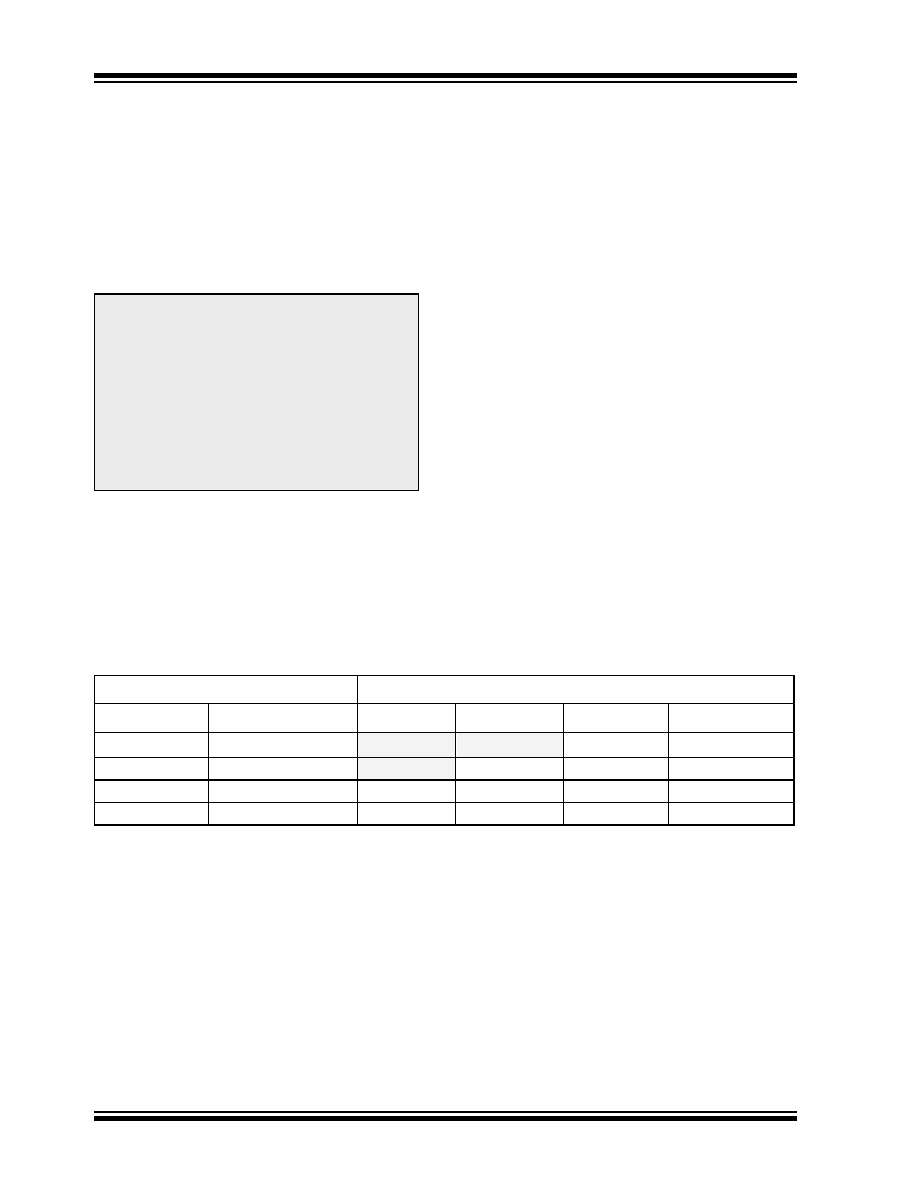
Note 1: The ADC operation is independent of the
state of the TRISB or ANSEL bits. These
bits must be configured by the firmware
prior to initiation of an ADC conversion.
2: When reading the PORTA or PORTB reg-
isters, all pins configured as analog input
channels will read as a ‘0’.
3: Analog levels on any pin that is defined as
a digital input, including AN<7:0>, may
cause the input buffer to consume excess
supply current.
ADC Clock Source (TAD)
Device Frequency
Operation
ADCS1:ADCS0
20 MHz
5 MHz
1.25 MHz
333.33kHz
2 TOSC
00
100 ns(2)
400 ns(2)
1.6 s
6
s
8 TOSC
01
400 ns
1.6
s6.4 s
24
s(3)
32 TOSC
10
1.6
s6.4 s25.6 s(3)
96
s(3)
RC
11
2 - 6
s(1,4)
2 - 6
s(1,4)
2 - 6
s(1,4)
2 - 6
s(1)
相关PDF资料 |
PDF描述 |
|---|---|
| PIC16LC715T-04I/SS | IC MCU OTP 2KX14 A/D PWM 20SSOP |
| W3L14C105MAT1A | CAP CER 1UF 4V 20% 4V X7R 0612 |
| PIC16LC63A-04/SP | IC MCU OTP 4KX14 PWM 28DIP |
| PIC16C56-LP/SO | IC MCU OTP 1KX12 18SOIC |
| FSA2567MPX | IC SWITCH 4PDT 16MLP |
相关代理商/技术参数 |
参数描述 |
|---|---|
| PIC16LC781T-I/SO | 功能描述:8位微控制器 -MCU 1.75KB 128RAM 16 I/O RoHS:否 制造商:Silicon Labs 核心:8051 处理器系列:C8051F39x 数据总线宽度:8 bit 最大时钟频率:50 MHz 程序存储器大小:16 KB 数据 RAM 大小:1 KB 片上 ADC:Yes 工作电源电压:1.8 V to 3.6 V 工作温度范围:- 40 C to + 105 C 封装 / 箱体:QFN-20 安装风格:SMD/SMT |
| PIC16LC781T-I/SS | 功能描述:8位微控制器 -MCU 1.75KB 128RAM 16 I/O Ind Temp SSOP20 RoHS:否 制造商:Silicon Labs 核心:8051 处理器系列:C8051F39x 数据总线宽度:8 bit 最大时钟频率:50 MHz 程序存储器大小:16 KB 数据 RAM 大小:1 KB 片上 ADC:Yes 工作电源电压:1.8 V to 3.6 V 工作温度范围:- 40 C to + 105 C 封装 / 箱体:QFN-20 安装风格:SMD/SMT |
| PIC16LC782-I/P | 功能描述:8位微控制器 -MCU 3.5KB 128 RAM 16 I/O RoHS:否 制造商:Silicon Labs 核心:8051 处理器系列:C8051F39x 数据总线宽度:8 bit 最大时钟频率:50 MHz 程序存储器大小:16 KB 数据 RAM 大小:1 KB 片上 ADC:Yes 工作电源电压:1.8 V to 3.6 V 工作温度范围:- 40 C to + 105 C 封装 / 箱体:QFN-20 安装风格:SMD/SMT |
| PIC16LC782-I/SO | 功能描述:8位微控制器 -MCU 3.5KB 128 RAM 16 I/O RoHS:否 制造商:Silicon Labs 核心:8051 处理器系列:C8051F39x 数据总线宽度:8 bit 最大时钟频率:50 MHz 程序存储器大小:16 KB 数据 RAM 大小:1 KB 片上 ADC:Yes 工作电源电压:1.8 V to 3.6 V 工作温度范围:- 40 C to + 105 C 封装 / 箱体:QFN-20 安装风格:SMD/SMT |
| PIC16LC782-I/SS | 功能描述:8位微控制器 -MCU 3.5KB 128 RAM 16 I/O RoHS:否 制造商:Silicon Labs 核心:8051 处理器系列:C8051F39x 数据总线宽度:8 bit 最大时钟频率:50 MHz 程序存储器大小:16 KB 数据 RAM 大小:1 KB 片上 ADC:Yes 工作电源电压:1.8 V to 3.6 V 工作温度范围:- 40 C to + 105 C 封装 / 箱体:QFN-20 安装风格:SMD/SMT |
发布紧急采购,3分钟左右您将得到回复。