- 您现在的位置:买卖IC网 > PDF目录11599 > PIC16LF1824-E/P (Microchip Technology)IC MCU 8BIT 7KB FLASH 14PDIP PDF资料下载
参数资料
| 型号: | PIC16LF1824-E/P |
| 厂商: | Microchip Technology |
| 文件页数: | 53/101页 |
| 文件大小: | 0K |
| 描述: | IC MCU 8BIT 7KB FLASH 14PDIP |
| 标准包装: | 30 |
| 系列: | PIC® XLP™ mTouch™ 16F |
| 核心处理器: | PIC |
| 芯体尺寸: | 8-位 |
| 速度: | 32MHz |
| 连通性: | I²C,SPI,UART/USART |
| 外围设备: | 欠压检测/复位,POR,PWM,WDT |
| 输入/输出数: | 11 |
| 程序存储器容量: | 7KB(4K x 14) |
| 程序存储器类型: | 闪存 |
| EEPROM 大小: | 256 x 8 |
| RAM 容量: | 256 x 8 |
| 电压 - 电源 (Vcc/Vdd): | 1.8 V ~ 3.6 V |
| 数据转换器: | A/D 8x10b |
| 振荡器型: | 内部 |
| 工作温度: | -40°C ~ 125°C |
| 封装/外壳: | 14-DIP(0.300",7.62mm) |
| 包装: | 管件 |
第1页第2页第3页第4页第5页第6页第7页第8页第9页第10页第11页第12页第13页第14页第15页第16页第17页第18页第19页第20页第21页第22页第23页第24页第25页第26页第27页第28页第29页第30页第31页第32页第33页第34页第35页第36页第37页第38页第39页第40页第41页第42页第43页第44页第45页第46页第47页第48页第49页第50页第51页第52页当前第53页第54页第55页第56页第57页第58页第59页第60页第61页第62页第63页第64页第65页第66页第67页第68页第69页第70页第71页第72页第73页第74页第75页第76页第77页第78页第79页第80页第81页第82页第83页第84页第85页第86页第87页第88页第89页第90页第91页第92页第93页第94页第95页第96页第97页第98页第99页第100页第101页
196
2552K–AVR–04/11
ATmega329/3290/649/6490
The 4-bit counter can be both read and written via the data bus, and can generate an overflow
interrupt. Both the Serial Register and the counter are clocked simultaneously by the same clock
source. This allows the counter to count the number of bits received or transmitted and generate
an interrupt when the transfer is complete. Note that when an external clock source is selected
the counter counts both clock edges. In this case the counter counts the number of edges, and
not the number of bits. The clock can be selected from three different sources: The USCK pin,
Timer/Counter0 Compare Match or from software.
The Two-wire clock control unit can generate an interrupt when a start condition is detected on
the Two-wire bus. It can also generate wait states by holding the clock pin low after a start con-
dition is detected, or after the counter overflows.
20.3
Functional Descriptions
20.3.1
Three-wire Mode
The USI Three-wire mode is compliant to the Serial Peripheral Interface (SPI) mode 0 and 1, but
does not have the slave select (SS) pin functionality. However, this feature can be implemented
in software if necessary. Pin names used by this mode are: DI, DO, and USCK.
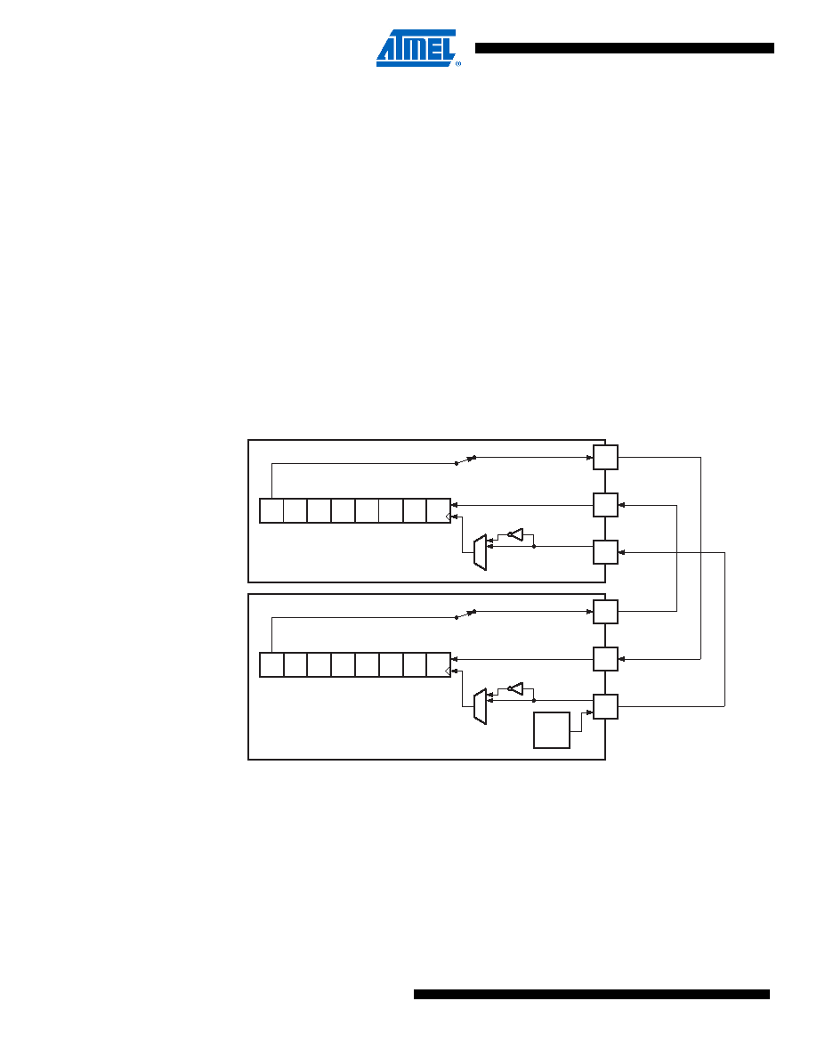
Figure 20-2. Three-wire Mode Operation, Simplified Diagram
Figure 20-2 shows two USI units operating in Three-wire mode, one as Master and one as
Slave. The two Shift Registers are interconnected in such way that after eight USCK clocks, the
data in each register are interchanged. The same clock also increments the USI’s 4-bit counter.
The Counter Overflow (interrupt) Flag, or USIOIF, can therefore be used to determine when a
transfer is completed. The clock is generated by the Master device software by toggling the
USCK pin via the PORT Register or by writing a one to the USITC bit in USICR.
SLAVE
MASTER
Bit7
Bit6
Bit5
Bit4
Bit3
Bit2
Bit1
Bit0
DO
DI
USCK
Bit7
Bit6
Bit5
Bit4
Bit3
Bit2
Bit1
Bit0
DO
DI
USCK
PORTxn
相关PDF资料 |
PDF描述 |
|---|---|
| PIC16F1824-E/P | IC MCU 8BIT 7KB FLASH 14PDIP |
| PIC16LF722A-E/SP | MCU 8BIT 2K FLASH XLP 28-SPDIP |
| PIC16F722A-E/SP | MCU 8BIT 2K FLASH XLP 28-SPDIP |
| PIC24F04KA200T-I/ST | IC PIC MCU FLASH 512KX4 14-TSSOP |
| PIC16F677T-I/SS | IC PIC MCU FLASH 2KX14 20SSOP |
相关代理商/技术参数 |
参数描述 |
|---|---|
| PIC16LF1824-I/ML | 功能描述:8位微控制器 -MCU 7KB Flash 256B RAM 32 MHz Int Osc Core RoHS:否 制造商:Silicon Labs 核心:8051 处理器系列:C8051F39x 数据总线宽度:8 bit 最大时钟频率:50 MHz 程序存储器大小:16 KB 数据 RAM 大小:1 KB 片上 ADC:Yes 工作电源电压:1.8 V to 3.6 V 工作温度范围:- 40 C to + 105 C 封装 / 箱体:QFN-20 安装风格:SMD/SMT |
| PIC16LF1824-I/P | 功能描述:8位微控制器 -MCU 7KB Flash 256B RAM 32 MHz Int Osc Core RoHS:否 制造商:Silicon Labs 核心:8051 处理器系列:C8051F39x 数据总线宽度:8 bit 最大时钟频率:50 MHz 程序存储器大小:16 KB 数据 RAM 大小:1 KB 片上 ADC:Yes 工作电源电压:1.8 V to 3.6 V 工作温度范围:- 40 C to + 105 C 封装 / 箱体:QFN-20 安装风格:SMD/SMT |
| PIC16LF1824-I/SL | 功能描述:8位微控制器 -MCU 7KB Flash 256B RAM 32 MHz Int Osc Core RoHS:否 制造商:Silicon Labs 核心:8051 处理器系列:C8051F39x 数据总线宽度:8 bit 最大时钟频率:50 MHz 程序存储器大小:16 KB 数据 RAM 大小:1 KB 片上 ADC:Yes 工作电源电压:1.8 V to 3.6 V 工作温度范围:- 40 C to + 105 C 封装 / 箱体:QFN-20 安装风格:SMD/SMT |
| PIC16LF1824-I/ST | 功能描述:8位微控制器 -MCU 7KB Flash 256B RAM 32 MHz Int Osc Core RoHS:否 制造商:Silicon Labs 核心:8051 处理器系列:C8051F39x 数据总线宽度:8 bit 最大时钟频率:50 MHz 程序存储器大小:16 KB 数据 RAM 大小:1 KB 片上 ADC:Yes 工作电源电压:1.8 V to 3.6 V 工作温度范围:- 40 C to + 105 C 封装 / 箱体:QFN-20 安装风格:SMD/SMT |
| PIC16LF1824T39A-I/ST | 制造商:Microchip Technology 功能描述:MCU 8-bit PIC16 PIC RISC 7KB Flash 2.5V/3.3V 20-Pin TSSOP 制造商:Microchip Technology Inc 功能描述:PIC16LF1824 MICROCONTROLLER WITH 300-900 MHZ TRANSMITTER - Rail/Tube 制造商:Microchip Technology Inc 功能描述:IC MCU 8BIT FLASH 20TSSOP 制造商:Microchip Technology Inc 功能描述:PIC16LF1824 Microcontroller |
发布紧急采购,3分钟左右您将得到回复。