- 您现在的位置:买卖IC网 > PDF目录11481 > PIC16LF628T-04/SS (Microchip Technology)IC MCU FLASH 2KX14 COMP 20SSOP PDF资料下载
参数资料
| 型号: | PIC16LF628T-04/SS |
| 厂商: | Microchip Technology |
| 文件页数: | 9/170页 |
| 文件大小: | 0K |
| 描述: | IC MCU FLASH 2KX14 COMP 20SSOP |
| 产品培训模块: | Asynchronous Stimulus |
| 标准包装: | 1,600 |
| 系列: | PIC® 16F |
| 核心处理器: | PIC |
| 芯体尺寸: | 8-位 |
| 速度: | 4MHz |
| 连通性: | UART/USART |
| 外围设备: | 欠压检测/复位,POR,PWM,WDT |
| 输入/输出数: | 16 |
| 程序存储器容量: | 3.5KB(2K x 14) |
| 程序存储器类型: | 闪存 |
| EEPROM 大小: | 128 x 8 |
| RAM 容量: | 224 x 8 |
| 电压 - 电源 (Vcc/Vdd): | 2 V ~ 5.5 V |
| 振荡器型: | 内部 |
| 工作温度: | 0°C ~ 70°C |
| 封装/外壳: | 20-SSOP(0.209",5.30mm 宽) |
| 包装: | 带卷 (TR) |
第1页第2页第3页第4页第5页第6页第7页第8页当前第9页第10页第11页第12页第13页第14页第15页第16页第17页第18页第19页第20页第21页第22页第23页第24页第25页第26页第27页第28页第29页第30页第31页第32页第33页第34页第35页第36页第37页第38页第39页第40页第41页第42页第43页第44页第45页第46页第47页第48页第49页第50页第51页第52页第53页第54页第55页第56页第57页第58页第59页第60页第61页第62页第63页第64页第65页第66页第67页第68页第69页第70页第71页第72页第73页第74页第75页第76页第77页第78页第79页第80页第81页第82页第83页第84页第85页第86页第87页第88页第89页第90页第91页第92页第93页第94页第95页第96页第97页第98页第99页第100页第101页第102页第103页第104页第105页第106页第107页第108页第109页第110页第111页第112页第113页第114页第115页第116页第117页第118页第119页第120页第121页第122页第123页第124页第125页第126页第127页第128页第129页第130页第131页第132页第133页第134页第135页第136页第137页第138页第139页第140页第141页第142页第143页第144页第145页第146页第147页第148页第149页第150页第151页第152页第153页第154页第155页第156页第157页第158页第159页第160页第161页第162页第163页第164页第165页第166页第167页第168页第169页第170页
PIC16F62X
DS40300C-page 104
Preliminary
2003 Microchip Technology Inc.
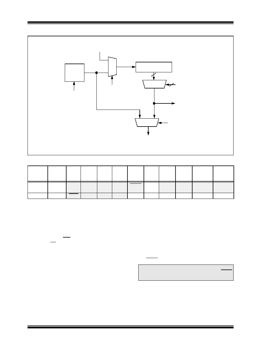
FIGURE 14-16:
WATCHDOG TIMER BLOCK DIAGRAM
TABLE 14-10: SUMMARY OF WATCHDOG TIMER REGISTERS
14.9
Power-Down Mode (SLEEP)
The Power-down mode is entered by executing a
SLEEP
instruction.
If enabled, the Watchdog Timer will be cleared but
keeps running, the PD bit in the STATUS register is
cleared, the TO bit is set, and the oscillator driver is
turned off. The I/O ports maintain the status they had,
before SLEEP was executed (driving high, low, or hi-
impedance).
For lowest current consumption in this mode, all I/O
pins should be either at V
DD, or VSS, with no external
circuitry drawing current from the I/O pin and the com-
parators, and V
REF should be disabled. I/O pins that
are hi-impedance inputs should be pulled high or low
externally to avoid switching currents caused by float-
ing inputs. The T0CKI input should also be at V
DD or
V
SS for lowest current consumption. The contribution
from on-chip pull-ups on PORTB should be considered.
The MCLR pin must be at a logic high level (V
IHMC).
Address
Name
Bit 7
Bit 6
Bit 5
Bit 4
Bit 3
Bit 2
Bit 1
Bit 0
Value on
POR Reset
Value on all
other
RESETS
2007h
Config.
bits
LVP
BODEN
MCLRE
FOSC2
PWRTE
WDTE
FOSC1
FOSC0
uuuu uuuu
81h
OPTION
RBPU
INTEDG
T0CS
T0SE
PSA
PS2
PS1
PS0
1111 1111
Legend:
_ = Unimplemented location, read as “0”, + = Reserved for future use
Note
1: Shaded cells are not used by the Watchdog Timer.
Note
1: T0SE, T0CS, PSA, PS0-PS2 are bits in the OPTION register.
From TMR0 Clock Source
Watchdog
Timer
WDT
Enable Bit
0
1
8
8 to 1 MUX
PS<2:0>
To TMR0
01
PSA
WDT
Timeout
PSA
M
U
X
MUX
3
WDT POSTSCALER/
TMR0 PRESCALER
Note:
It should be noted that a RESET generated
by a WDT timeout does not drive MCLR
pin low.
相关PDF资料 |
PDF描述 |
|---|---|
| VI-B30-IY-B1 | CONVERTER MOD DC/DC 5V 50W |
| PIC16CE625T-04/SO | IC MCU OTP 2KX14 EE COMP 18SOIC |
| ADG508FBNZ | IC MULTIPLEXER 8X1 16DIP |
| VI-B2Z-IX-B1 | CONVERTER MOD DC/DC 2V 30W |
| PIC16F946T-I/PT | IC PIC MCU FLASH 8KX14 64TQFP |
相关代理商/技术参数 |
参数描述 |
|---|---|
| PIC16LF648A-I/ML | 功能描述:8位微控制器 -MCU 7KB 256 RAM 16 I/O RoHS:否 制造商:Silicon Labs 核心:8051 处理器系列:C8051F39x 数据总线宽度:8 bit 最大时钟频率:50 MHz 程序存储器大小:16 KB 数据 RAM 大小:1 KB 片上 ADC:Yes 工作电源电压:1.8 V to 3.6 V 工作温度范围:- 40 C to + 105 C 封装 / 箱体:QFN-20 安装风格:SMD/SMT |
| PIC16LF648A-I/P | 功能描述:8位微控制器 -MCU 7KB 256 RAM 16 I/O RoHS:否 制造商:Silicon Labs 核心:8051 处理器系列:C8051F39x 数据总线宽度:8 bit 最大时钟频率:50 MHz 程序存储器大小:16 KB 数据 RAM 大小:1 KB 片上 ADC:Yes 工作电源电压:1.8 V to 3.6 V 工作温度范围:- 40 C to + 105 C 封装 / 箱体:QFN-20 安装风格:SMD/SMT |
| PIC16LF648A-I/SO | 功能描述:8位微控制器 -MCU 7KB 256 RAM 16 I/O RoHS:否 制造商:Silicon Labs 核心:8051 处理器系列:C8051F39x 数据总线宽度:8 bit 最大时钟频率:50 MHz 程序存储器大小:16 KB 数据 RAM 大小:1 KB 片上 ADC:Yes 工作电源电压:1.8 V to 3.6 V 工作温度范围:- 40 C to + 105 C 封装 / 箱体:QFN-20 安装风格:SMD/SMT |
| PIC16LF648A-I/SO | 制造商:Microchip Technology Inc 功能描述:IC 8BIT MCU PIC16LF 20MHZ SOIC-18 |
| PIC16LF648A-I/SOG | 功能描述:8位微控制器 -MCU 7kBF 256RM 16I/O Lead Free Package RoHS:否 制造商:Silicon Labs 核心:8051 处理器系列:C8051F39x 数据总线宽度:8 bit 最大时钟频率:50 MHz 程序存储器大小:16 KB 数据 RAM 大小:1 KB 片上 ADC:Yes 工作电源电压:1.8 V to 3.6 V 工作温度范围:- 40 C to + 105 C 封装 / 箱体:QFN-20 安装风格:SMD/SMT |
发布紧急采购,3分钟左右您将得到回复。