- 您现在的位置:买卖IC网 > PDF目录11509 > PIC16LF72T-I/SS (Microchip Technology)IC MCU FLASH 2KX14 LV AD 28-SSOP PDF资料下载
参数资料
| 型号: | PIC16LF72T-I/SS |
| 厂商: | Microchip Technology |
| 文件页数: | 136/136页 |
| 文件大小: | 0K |
| 描述: | IC MCU FLASH 2KX14 LV AD 28-SSOP |
| 产品培训模块: | Asynchronous Stimulus |
| 标准包装: | 2,100 |
| 系列: | PIC® 16F |
| 核心处理器: | PIC |
| 芯体尺寸: | 8-位 |
| 速度: | 20MHz |
| 连通性: | I²C,SPI |
| 外围设备: | 欠压检测/复位,POR,PWM,WDT |
| 输入/输出数: | 22 |
| 程序存储器容量: | 3.5KB(2K x 14) |
| 程序存储器类型: | 闪存 |
| RAM 容量: | 128 x 8 |
| 电压 - 电源 (Vcc/Vdd): | 2 V ~ 5.5 V |
| 数据转换器: | A/D 5x8b |
| 振荡器型: | 外部 |
| 工作温度: | -40°C ~ 85°C |
| 封装/外壳: | 28-SSOP(0.209",5.30mm 宽) |
| 包装: | 带卷 (TR) |
第1页第2页第3页第4页第5页第6页第7页第8页第9页第10页第11页第12页第13页第14页第15页第16页第17页第18页第19页第20页第21页第22页第23页第24页第25页第26页第27页第28页第29页第30页第31页第32页第33页第34页第35页第36页第37页第38页第39页第40页第41页第42页第43页第44页第45页第46页第47页第48页第49页第50页第51页第52页第53页第54页第55页第56页第57页第58页第59页第60页第61页第62页第63页第64页第65页第66页第67页第68页第69页第70页第71页第72页第73页第74页第75页第76页第77页第78页第79页第80页第81页第82页第83页第84页第85页第86页第87页第88页第89页第90页第91页第92页第93页第94页第95页第96页第97页第98页第99页第100页第101页第102页第103页第104页第105页第106页第107页第108页第109页第110页第111页第112页第113页第114页第115页第116页第117页第118页第119页第120页第121页第122页第123页第124页第125页第126页第127页第128页第129页第130页第131页第132页第133页第134页第135页当前第136页
99
2535J–AVR–08/10
ATtiny13
The LPM instruction uses the Z-pointer to store the address. Since this instruction addresses the
Flash byte-by-byte, also the LSB (bit Z0) of the Z-pointer is used.
16.5 EEPROM Write Prevents Writing to SPMCSR
Note that an EEPROM write operation will block all software programming to Flash. Reading the
fuses and lock bits from software will also be prevented during the EEPROM write operation. It is
recommended that the user checks the status bit (EEPE) in the EECR Register and verifies that
the bit is cleared before writing to the SPMCSR Register.
16.6 Reading Fuse and Lock Bits from Firmware
It is possible to read fuse and lock bits from software.
16.6.1
Reading Lock Bits from Firmware
Issuing an LPM instruction within three CPU cycles after RFLB and SELFPRGEN bits have
been set in SPMCSR will return lock bit values in the destination register. The RFLB and SELF-
PRGEN bits automatically clear upon completion of reading the lock bits, or if no LPM instruction
is executed within three CPU cycles, or if no SPM instruction is executed within four CPU cycles.
When RFLB and SELFPRGEN are cleared, LPM functions normally.
To read the lock bits, follow the below procedure.
1. Load the Z-pointer with 0x0001.
2. Set RFLB and SELFPRGEN bits in SPMCSR.
3. Issuing an LPM instruction within three clock cycles will return lock bits in the destina-
tion register.
If successful, the contents of the destination register are as follows.
See section “Program And Data Memory Lock Bits” on page 102 for more information on lock
bits.
16.6.2
Reading Fuse Bits from Firmware
The algorithm for reading fuse bytes is similar to the one described above for reading lock bits,
only the addresses are different.
To read the Fuse Low Byte (FLB), follow the below procedure:
1. Load the Z-pointer with 0x0000.
2. Set RFLB and SELFPRGEN bits in SPMCSR.
3. Issuing an LPM instruction within three clock cycles will FLB in the destination register.
If successful, the contents of the destination register are as follows.
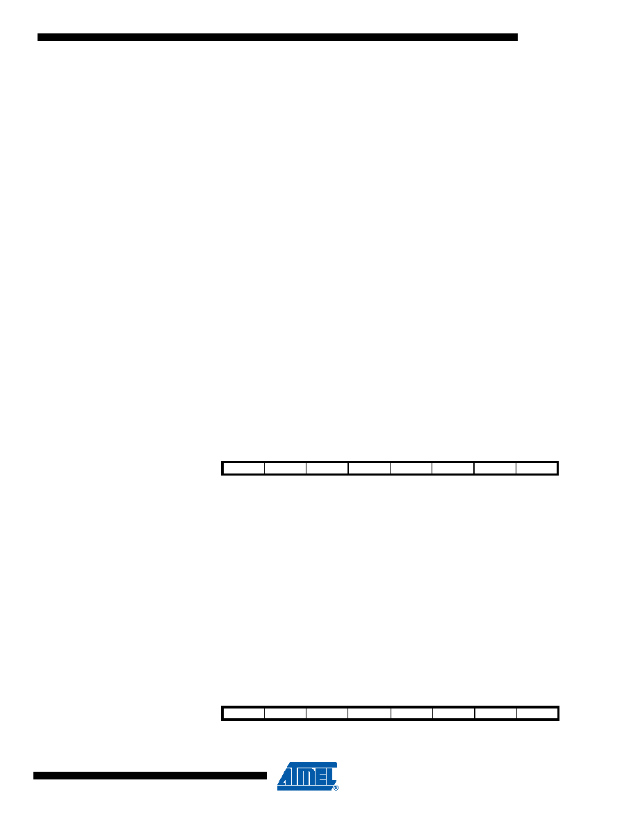
Bit
7
654321
0
Rd
–
–––––
LB2
LB1
Bit
7
6
543
2
1
0
Rd
FLB7
FLB6
FLB5
FLB4
FLB3
FLB2
FLB1
FLB0
相关PDF资料 |
PDF描述 |
|---|---|
| PIC16CE623-04I/SS | IC MCU OTP 512X14 EE COMP 20SSOP |
| MRF01J-HRMJ | CONN ADAPTER MRF01 JACK-SMA JACK |
| VI-BTY-IX-B1 | CONVERTER MOD DC/DC 3.3V 49.5W |
| HRMP-W.FLJ | RF CONN CONVERSION ADAPTER |
| VI-BTX-IY-B1 | CONVERTER MOD DC/DC 5.2V 50W |
相关代理商/技术参数 |
参数描述 |
|---|---|
| PIC16LF737-I/ML | 功能描述:8位微控制器 -MCU 7KB 368 RAM 25 I/O RoHS:否 制造商:Silicon Labs 核心:8051 处理器系列:C8051F39x 数据总线宽度:8 bit 最大时钟频率:50 MHz 程序存储器大小:16 KB 数据 RAM 大小:1 KB 片上 ADC:Yes 工作电源电压:1.8 V to 3.6 V 工作温度范围:- 40 C to + 105 C 封装 / 箱体:QFN-20 安装风格:SMD/SMT |
| PIC16LF737-I/SO | 功能描述:8位微控制器 -MCU 7KB 368 RAM 25 I/O RoHS:否 制造商:Silicon Labs 核心:8051 处理器系列:C8051F39x 数据总线宽度:8 bit 最大时钟频率:50 MHz 程序存储器大小:16 KB 数据 RAM 大小:1 KB 片上 ADC:Yes 工作电源电压:1.8 V to 3.6 V 工作温度范围:- 40 C to + 105 C 封装 / 箱体:QFN-20 安装风格:SMD/SMT |
| PIC16LF737-I/SP | 功能描述:8位微控制器 -MCU 7KB 368 RAM 25 I/O RoHS:否 制造商:Silicon Labs 核心:8051 处理器系列:C8051F39x 数据总线宽度:8 bit 最大时钟频率:50 MHz 程序存储器大小:16 KB 数据 RAM 大小:1 KB 片上 ADC:Yes 工作电源电压:1.8 V to 3.6 V 工作温度范围:- 40 C to + 105 C 封装 / 箱体:QFN-20 安装风格:SMD/SMT |
| PIC16LF737-I/SS | 功能描述:8位微控制器 -MCU 7KB 368 RAM 25 I/O RoHS:否 制造商:Silicon Labs 核心:8051 处理器系列:C8051F39x 数据总线宽度:8 bit 最大时钟频率:50 MHz 程序存储器大小:16 KB 数据 RAM 大小:1 KB 片上 ADC:Yes 工作电源电压:1.8 V to 3.6 V 工作温度范围:- 40 C to + 105 C 封装 / 箱体:QFN-20 安装风格:SMD/SMT |
| PIC16LF737T-I/ML | 功能描述:8位微控制器 -MCU 7KB 368 RAM 25 I/O RoHS:否 制造商:Silicon Labs 核心:8051 处理器系列:C8051F39x 数据总线宽度:8 bit 最大时钟频率:50 MHz 程序存储器大小:16 KB 数据 RAM 大小:1 KB 片上 ADC:Yes 工作电源电压:1.8 V to 3.6 V 工作温度范围:- 40 C to + 105 C 封装 / 箱体:QFN-20 安装风格:SMD/SMT |
发布紧急采购,3分钟左右您将得到回复。