- 您现在的位置:买卖IC网 > PDF目录11232 > PIC17C766-16I/L (Microchip Technology)IC MCU OTP 16KX16 A/D 84PLCC PDF资料下载
参数资料
| 型号: | PIC17C766-16I/L |
| 厂商: | Microchip Technology |
| 文件页数: | 94/159页 |
| 文件大小: | 0K |
| 描述: | IC MCU OTP 16KX16 A/D 84PLCC |
| 产品培训模块: | Asynchronous Stimulus |
| 标准包装: | 16 |
| 系列: | PIC® 17C |
| 核心处理器: | PIC |
| 芯体尺寸: | 8-位 |
| 速度: | 16MHz |
| 连通性: | I²C,SPI,UART/USART |
| 外围设备: | 欠压检测/复位,POR,PWM,WDT |
| 输入/输出数: | 66 |
| 程序存储器容量: | 32KB(16K x 16) |
| 程序存储器类型: | OTP |
| RAM 容量: | 902 x 8 |
| 电压 - 电源 (Vcc/Vdd): | 4.5 V ~ 5.5 V |
| 数据转换器: | A/D 16x10b |
| 振荡器型: | 外部 |
| 工作温度: | -40°C ~ 85°C |
| 封装/外壳: | 84-LCC(J 形引线) |
| 包装: | 管件 |
| 配用: | AC164318-ND - MODULE SKT MPLAB PM3 84PLCC DVA17XL841-ND - DEVICE ADAPTER FOR PIC17C762 DM173001-ND - KIT DEVELOPMENT PICDEM17 AC164027-ND - ADAPTER PICSTART PLUS 84PLCC AC174012-ND - MODULE SKT PROMATEII 84PLCC |
第1页第2页第3页第4页第5页第6页第7页第8页第9页第10页第11页第12页第13页第14页第15页第16页第17页第18页第19页第20页第21页第22页第23页第24页第25页第26页第27页第28页第29页第30页第31页第32页第33页第34页第35页第36页第37页第38页第39页第40页第41页第42页第43页第44页第45页第46页第47页第48页第49页第50页第51页第52页第53页第54页第55页第56页第57页第58页第59页第60页第61页第62页第63页第64页第65页第66页第67页第68页第69页第70页第71页第72页第73页第74页第75页第76页第77页第78页第79页第80页第81页第82页第83页第84页第85页第86页第87页第88页第89页第90页第91页第92页第93页当前第94页第95页第96页第97页第98页第99页第100页第101页第102页第103页第104页第105页第106页第107页第108页第109页第110页第111页第112页第113页第114页第115页第116页第117页第118页第119页第120页第121页第122页第123页第124页第125页第126页第127页第128页第129页第130页第131页第132页第133页第134页第135页第136页第137页第138页第139页第140页第141页第142页第143页第144页第145页第146页第147页第148页第149页第150页第151页第152页第153页第154页第155页第156页第157页第158页第159页
2000 Microchip Technology Inc.
DS30289B-page 39
PIC17C7XX
6.4
Interrupt Operation
Global Interrupt Disable bit, GLINTD (CPUSTA<4>),
enables all unmasked interrupts (if clear), or disables
all interrupts (if set). Individual interrupts can be dis-
abled through their corresponding enable bits in the
INTSTA register. Peripheral interrupts need either the
global peripheral enable PEIE bit disabled, or the spe-
cific peripheral enable bit disabled. Disabling the
peripherals via the global peripheral enable bit, dis-
ables all peripheral interrupts. GLINTD is set on
RESET (interrupts disabled).
The RETFIE instruction clears the GLINTD bit while
forcing the Program Counter (PC) to the value loaded
at the Top-of-Stack.
When an interrupt is responded to, the GLINTD bit is
automatically set to disable any further interrupt, the
return address is pushed onto the stack and the PC is
loaded with the interrupt vector. There are four interrupt
vectors which help reduce interrupt latency.
The peripheral interrupt vector has multiple interrupt
sources. Once in the peripheral Interrupt Service Rou-
tine, the source(s) of the interrupt can be determined by
polling the interrupt flag bits. The peripheral interrupt
flag bit(s) must be cleared in software before re-
enabling interrupts to avoid continuous interrupts.
The PIC17C7XX devices have four interrupt vectors.
These vectors and their hardware priority are shown in
Table 6-1. If two enabled interrupts occur “at the same
time”, the interrupt of the highest priority will be ser-
viced first. This means that the vector address of that
interrupt will be loaded into the program counter (PC).
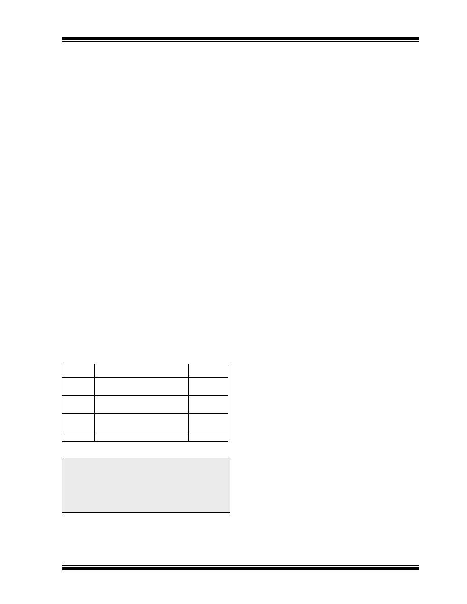
TABLE 6-1:
INTERRUPT VECTORS/
PRIORITIES
6.5
RA0/INT Interrupt
The external interrupt on the RA0/INT pin is edge trig-
gered. Either the rising edge if the INTEDG bit
(T0STA<7>) is set, or the falling edge if the INTEDG bit
is clear. When a valid edge appears on the RA0/INT
pin, the INTF bit (INTSTA<4>) is set. This interrupt can
be
disabled
by
clearing
the
INTE
control
bit
(INTSTA<0>). The INT interrupt can wake the proces-
sor from SLEEP. See Section 17.4 for details on
SLEEP operation.
6.6
T0CKI Interrupt
The external interrupt on the RA1/T0CKI pin is edge
triggered. Either the rising edge if the T0SE bit
(T0STA<6>) is set, or the falling edge if the T0SE bit is
clear. When a valid edge appears on the RA1/T0CKI
pin, the T0CKIF bit (INTSTA<6>) is set. This interrupt
can be disabled by clearing the T0CKIE control bit
(INTSTA<2>). The T0CKI interrupt can wake up the
processor from SLEEP. See Section 17.4 for details on
SLEEP operation.
6.7
Peripheral Interrupt
The peripheral interrupt flag indicates that at least one
of the peripheral interrupts occurred (PEIF is set). The
PEIF bit is a read only bit and is a bit wise OR of all the
flag bits in the PIR registers AND’d with the correspond-
ing enable bits in the PIE registers. Some of the periph-
eral interrupts can wake the processor from SLEEP.
See Section 17.4 for details on SLEEP operation.
6.8
Context Saving During Interrupts
During an interrupt, only the returned PC value is saved
on the stack. Typically, users may wish to save key reg-
isters during an interrupt; e.g. WREG, ALUSTA and the
BSR registers. This requires implementation in software.
Example 6-2 shows the saving and restoring of infor-
mation for an Interrupt Service Routine. This is for a
simple interrupt scheme, where only one interrupt may
occur at a time (no interrupt nesting). The SFRs are
stored in the non-banked GPR area.
Example 6-2 shows the saving and restoring of infor-
mation for a more complex Interrupt Service Routine.
This is useful where nesting of interrupts is required. A
maximum of 6 levels can be done by this example. The
BSR is stored in the non-banked GPR area, while the
other registers would be stored in a particular bank.
Therefore, 6 saves may be done with this routine (since
there are 6 non-banked GPR registers). These routines
require a dedicated indirect addressing register, FSR0,
to be selected for this.
The PUSH and POP code segments could either be in
each Interrupt Service Routine, or could be subroutines
that were called. Depending on the application, other
registers may also need to be saved.
Address
Vector
Priority
0008h
External Interrupt on RA0/
INT pin (INTF)
1 (Highest)
0010h
TMR0 Overflow Interrupt
(T0IF)
2
0018h
External Interrupt on T0CKI
(T0CKIF)
3
0020h
Peripherals (PEIF)
4 (Lowest)
Note 1: Individual interrupt flag bits are set, regard-
less of the status of their corresponding
mask bit or the GLINTD bit.
2: Before disabling any of the INTSTA enable
bits, the GLINTD bit should be set
(disabled).
相关PDF资料 |
PDF描述 |
|---|---|
| ADG904BCPZ | IC MULTIPLEXER 4X1 20LFCSP |
| ADG904BRUZ-R | IC MULTIPLEXER 4X1 20TSSOP |
| ADG1233YCPZ-REEL | IC SWITCH TRIPLE SPDT 16LFCSP |
| AD8195ACPZ-R7 | IC BUFF HDMI/DVI W/EQUAL 40LFCSP |
| M39014/02-1310V | CAP CER 100000PF 10% 100V RAD |
相关代理商/技术参数 |
参数描述 |
|---|---|
| PIC17C766-33/L | 功能描述:8位微控制器 -MCU 32KB 902 RAM 66 I/O RoHS:否 制造商:Silicon Labs 核心:8051 处理器系列:C8051F39x 数据总线宽度:8 bit 最大时钟频率:50 MHz 程序存储器大小:16 KB 数据 RAM 大小:1 KB 片上 ADC:Yes 工作电源电压:1.8 V to 3.6 V 工作温度范围:- 40 C to + 105 C 封装 / 箱体:QFN-20 安装风格:SMD/SMT |
| PIC17C766-33/L | 制造商:Microchip Technology Inc 功能描述:8BIT CMOS MCU SMD 17C766 PLCC84 |
| PIC17C766-33/PT | 功能描述:8位微控制器 -MCU 32KB 902 RAM 66 I/O RoHS:否 制造商:Silicon Labs 核心:8051 处理器系列:C8051F39x 数据总线宽度:8 bit 最大时钟频率:50 MHz 程序存储器大小:16 KB 数据 RAM 大小:1 KB 片上 ADC:Yes 工作电源电压:1.8 V to 3.6 V 工作温度范围:- 40 C to + 105 C 封装 / 箱体:QFN-20 安装风格:SMD/SMT |
| PIC17C766-33E/L | 功能描述:8位微控制器 -MCU 32KB 902 RAM 66 I/O RoHS:否 制造商:Silicon Labs 核心:8051 处理器系列:C8051F39x 数据总线宽度:8 bit 最大时钟频率:50 MHz 程序存储器大小:16 KB 数据 RAM 大小:1 KB 片上 ADC:Yes 工作电源电压:1.8 V to 3.6 V 工作温度范围:- 40 C to + 105 C 封装 / 箱体:QFN-20 安装风格:SMD/SMT |
| PIC17C766-33E/PT | 功能描述:8位微控制器 -MCU 32KB 902 RAM 66 I/O RoHS:否 制造商:Silicon Labs 核心:8051 处理器系列:C8051F39x 数据总线宽度:8 bit 最大时钟频率:50 MHz 程序存储器大小:16 KB 数据 RAM 大小:1 KB 片上 ADC:Yes 工作电源电压:1.8 V to 3.6 V 工作温度范围:- 40 C to + 105 C 封装 / 箱体:QFN-20 安装风格:SMD/SMT |
发布紧急采购,3分钟左右您将得到回复。