- 您现在的位置:买卖IC网 > PDF目录11557 > PIC18F14K50T-I/SS (Microchip Technology)IC PIC MCU FLASH 8KX8 20-SSOP PDF资料下载
参数资料
| 型号: | PIC18F14K50T-I/SS |
| 厂商: | Microchip Technology |
| 文件页数: | 93/285页 |
| 文件大小: | 0K |
| 描述: | IC PIC MCU FLASH 8KX8 20-SSOP |
| 视频文件: | World's Lowest Power in Sleep MCU: nanoWatt XLP |
| 标准包装: | 1,600 |
| 系列: | PIC® XLP™ 18F |
| 核心处理器: | PIC |
| 芯体尺寸: | 8-位 |
| 速度: | 48MHz |
| 连通性: | I²C,SPI,UART/USART,USB |
| 外围设备: | 欠压检测/复位,POR,PWM,WDT |
| 输入/输出数: | 14 |
| 程序存储器容量: | 16KB(8K x 16) |
| 程序存储器类型: | 闪存 |
| EEPROM 大小: | 256 x 8 |
| RAM 容量: | 768 x 8 |
| 电压 - 电源 (Vcc/Vdd): | 1.8 V ~ 5.5 V |
| 数据转换器: | A/D 11x10b |
| 振荡器型: | 内部 |
| 工作温度: | -40°C ~ 85°C |
| 封装/外壳: | 20-SSOP(0.209",5.30mm 宽) |
| 包装: | 带卷 (TR) |
| 配用: | AC244023-ND - PROC EXTENS PAK PIC18F1XK50 DV164126-ND - KIT DEVELOPMENT USB W/PICKIT 2 DM164127-ND - KIT DEVELOPMENT USB 18F14/13K50 AC164112-ND - VOLTAGE LIMITER MPLAB ICD2 VPP |
第1页第2页第3页第4页第5页第6页第7页第8页第9页第10页第11页第12页第13页第14页第15页第16页第17页第18页第19页第20页第21页第22页第23页第24页第25页第26页第27页第28页第29页第30页第31页第32页第33页第34页第35页第36页第37页第38页第39页第40页第41页第42页第43页第44页第45页第46页第47页第48页第49页第50页第51页第52页第53页第54页第55页第56页第57页第58页第59页第60页第61页第62页第63页第64页第65页第66页第67页第68页第69页第70页第71页第72页第73页第74页第75页第76页第77页第78页第79页第80页第81页第82页第83页第84页第85页第86页第87页第88页第89页第90页第91页第92页当前第93页第94页第95页第96页第97页第98页第99页第100页第101页第102页第103页第104页第105页第106页第107页第108页第109页第110页第111页第112页第113页第114页第115页第116页第117页第118页第119页第120页第121页第122页第123页第124页第125页第126页第127页第128页第129页第130页第131页第132页第133页第134页第135页第136页第137页第138页第139页第140页第141页第142页第143页第144页第145页第146页第147页第148页第149页第150页第151页第152页第153页第154页第155页第156页第157页第158页第159页第160页第161页第162页第163页第164页第165页第166页第167页第168页第169页第170页第171页第172页第173页第174页第175页第176页第177页第178页第179页第180页第181页第182页第183页第184页第185页第186页第187页第188页第189页第190页第191页第192页第193页第194页第195页第196页第197页第198页第199页第200页第201页第202页第203页第204页第205页第206页第207页第208页第209页第210页第211页第212页第213页第214页第215页第216页第217页第218页第219页第220页第221页第222页第223页第224页第225页第226页第227页第228页第229页第230页第231页第232页第233页第234页第235页第236页第237页第238页第239页第240页第241页第242页第243页第244页第245页第246页第247页第248页第249页第250页第251页第252页第253页第254页第255页第256页第257页第258页第259页第260页第261页第262页第263页第264页第265页第266页第267页第268页第269页第270页第271页第272页第273页第274页第275页第276页第277页第278页第279页第280页第281页第282页第283页第284页第285页
2006 Microchip Technology Inc.
Preliminary
DS70178C-page 181
dsPIC30F1010/202X
16.4
ADC Result Buffer
The ADC module contains up to 12 data output regis-
ters to store the A/D results called ADCBUF<11:0>.
The registers are 10 bits wide, but are read into differ-
ent format, 16-bit words. The buffers are read-only.
Each analog input has a corresponding data
output register.
This module DOES NOT include a circular data
buffer or FIFO. Because the conversion results may
be produced in any order, such schemes will not work
since there would be no means to determine which
data is in a specific location.
The SAR write to the buffers is synchronous to the
ADC clock. Reads from the buffers will always have
valid data assuming that the data-ready interrupt has
been processed.
If a buffer location has not been read by the software
and the SAR needs to overwrite that location, the
previous data is lost.
Reads from the result buffer pass through the data for-
matter. The 10 bits of the result data are formatted into
a 16-bit word.
16.5
Application Information
The ADC module implements a concept based on
“Conversion Pairs”. In power conversion applications,
there is a need to measure voltages and currents for
each PWM control loop. The ADC module enables the
sample and conversion process of each conversion
pair to be precisely timed relative to the PWM signals.
In a user’s application circuit, the PWM signal enables
a transistor, which allows an inductor to charge up with
current to a desired value. The longer a PWM signal is
on, the longer the inductor is charging, and therefore
the inductor current is at its maximum at the end of the
PWM signal. Often, this is the point where the user
wants to take the current and voltage measurements.
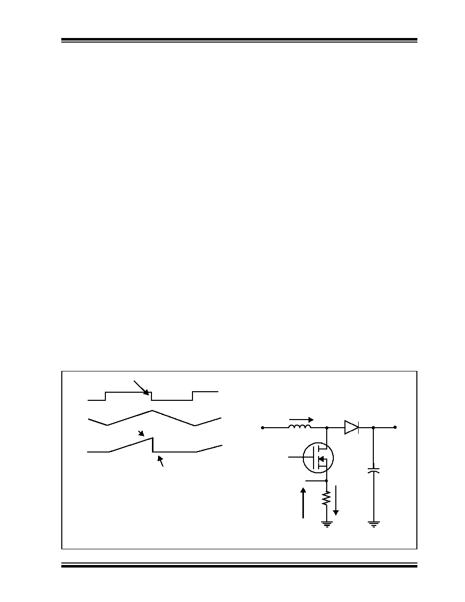
Figure 16-2 shows a typical power conversion applica-
tion (a boost converter) where the current sensing of
the inductor is done by monitoring the voltage across a
resistor in series with the power transistor that
“charges” the inductor. The significant feature of this
figure is that if the sampling of the resistor voltage
occurs slightly later than the desired sample point, the
data read will be zero. This is not acceptable in most
applications. The ADC module always samples the
analog voltages at the appointed time regardless of
whether the ADC converter is busy or not.
The Power Supply PWM module supports 2-4 indepen-
dent PWM channels as well as 2-4 trigger signals (one
per PWM generator). The user can configure these
channels to initiate an ADC conversion of a selected
input pair at the proper time in the PWM cycle. The
Power Supply PWM module also provides an addi-
tional trigger signal (Special Event Trigger), which can
be programmed to occur at a specified time during the
primary time base count cycle.
FIGURE 16-2:
APPLICATION EXAMPLE: IMPORTANCE OF PRECISE SAMPLING
X
PWM
IL
IR
X
Late sample yields
zero data
Desired sample point
Critical Edge
+VIN
IL
L
PWM
VISENSE
VOUT
COUT
+
IR
R
Measuring peak inductor current is very important
Example Boost Converter
相关PDF资料 |
PDF描述 |
|---|---|
| V375A36C400B | CONVERTER MOD DC/DC 36V 400W |
| V375C48M75BG3 | CONVERTER MOD DC/DC 48V 75W |
| 1-413589-4 | CONN PLUG BNC JIS 3C-2W CRIMP AU |
| V375C48M75BG2 | CONVERTER MOD DC/DC 48V 75W |
| PIC16LF726-E/ML | IC PIC MCU FLASH 8KX14 28-QFN |
相关代理商/技术参数 |
参数描述 |
|---|---|
| PIC18F2220-E/SO | 功能描述:8位微控制器 -MCU 4KB 512 RAM 25 I/O RoHS:否 制造商:Silicon Labs 核心:8051 处理器系列:C8051F39x 数据总线宽度:8 bit 最大时钟频率:50 MHz 程序存储器大小:16 KB 数据 RAM 大小:1 KB 片上 ADC:Yes 工作电源电压:1.8 V to 3.6 V 工作温度范围:- 40 C to + 105 C 封装 / 箱体:QFN-20 安装风格:SMD/SMT |
| PIC18F2220-E/SP | 功能描述:8位微控制器 -MCU 4KB 512 RAM 25 I/O RoHS:否 制造商:Silicon Labs 核心:8051 处理器系列:C8051F39x 数据总线宽度:8 bit 最大时钟频率:50 MHz 程序存储器大小:16 KB 数据 RAM 大小:1 KB 片上 ADC:Yes 工作电源电压:1.8 V to 3.6 V 工作温度范围:- 40 C to + 105 C 封装 / 箱体:QFN-20 安装风格:SMD/SMT |
| PIC18F2220-I/SO | 功能描述:8位微控制器 -MCU 4KB 512 RAM 25 I/O RoHS:否 制造商:Silicon Labs 核心:8051 处理器系列:C8051F39x 数据总线宽度:8 bit 最大时钟频率:50 MHz 程序存储器大小:16 KB 数据 RAM 大小:1 KB 片上 ADC:Yes 工作电源电压:1.8 V to 3.6 V 工作温度范围:- 40 C to + 105 C 封装 / 箱体:QFN-20 安装风格:SMD/SMT |
| PIC18F2220-I/SO | 制造商:Microchip Technology Inc 功能描述:IC 8BIT FLASH MCU 18F2220 SOIC28 |
| PIC18F2220-I/SOC03 | 制造商:Microchip Technology Inc 功能描述: |
发布紧急采购,3分钟左右您将得到回复。