- 您现在的位置:买卖IC网 > PDF目录11288 > PIC18F458T-I/PT (Microchip Technology)IC MCU FLASH 16KX16 W/CAN 44TQFP PDF资料下载
参数资料
| 型号: | PIC18F458T-I/PT |
| 厂商: | Microchip Technology |
| 文件页数: | 88/116页 |
| 文件大小: | 0K |
| 描述: | IC MCU FLASH 16KX16 W/CAN 44TQFP |
| 产品培训模块: | Asynchronous Stimulus |
| 标准包装: | 1,200 |
| 系列: | PIC® 18F |
| 核心处理器: | PIC |
| 芯体尺寸: | 8-位 |
| 速度: | 40MHz |
| 连通性: | CAN,I²C,SPI,UART/USART |
| 外围设备: | 欠压检测/复位,LVD,POR,PWM,WDT |
| 输入/输出数: | 33 |
| 程序存储器容量: | 32KB(16K x 16) |
| 程序存储器类型: | 闪存 |
| EEPROM 大小: | 256 x 8 |
| RAM 容量: | 1.5K x 8 |
| 电压 - 电源 (Vcc/Vdd): | 4.2 V ~ 5.5 V |
| 数据转换器: | A/D 8x10b |
| 振荡器型: | 外部 |
| 工作温度: | -40°C ~ 85°C |
| 封装/外壳: | 44-TQFP |
| 包装: | 带卷 (TR) |
第1页第2页第3页第4页第5页第6页第7页第8页第9页第10页第11页第12页第13页第14页第15页第16页第17页第18页第19页第20页第21页第22页第23页第24页第25页第26页第27页第28页第29页第30页第31页第32页第33页第34页第35页第36页第37页第38页第39页第40页第41页第42页第43页第44页第45页第46页第47页第48页第49页第50页第51页第52页第53页第54页第55页第56页第57页第58页第59页第60页第61页第62页第63页第64页第65页第66页第67页第68页第69页第70页第71页第72页第73页第74页第75页第76页第77页第78页第79页第80页第81页第82页第83页第84页第85页第86页第87页当前第88页第89页第90页第91页第92页第93页第94页第95页第96页第97页第98页第99页第100页第101页第102页第103页第104页第105页第106页第107页第108页第109页第110页第111页第112页第113页第114页第115页第116页
2006 Microchip Technology Inc.
DS41159E-page 71
PIC18FXX8
6.5
Writing to Flash Program Memory
The minimum programming block is 4 words or 8 bytes.
Word or byte programming is not supported.
Table writes are used internally to load the holding
registers needed to program the Flash memory. There
are 8 holding registers used by the table writes for
programming.
Since the Table Latch (TABLAT) is only a single byte,
the TBLWT instruction has to be executed 8 times for
each programming operation. All of the table write
operations will essentially be short writes, because only
the holding registers are written. At the end of updating
8 registers, the EECON1 register must be written to, to
start the programming operation with a long write.
The long write is necessary for programming the inter-
nal Flash. Instruction execution is halted while in a long
write cycle. The long write will be terminated by the
internal programming timer.
The EEPROM on-chip timer controls the write time.
The write/erase voltages are generated by an on-chip
charge pump rated to operate over the voltage range of
the device for byte or word operations.
6.5.1
FLASH PROGRAM MEMORY WRITE
SEQUENCE
The sequence of events for programming an internal
program memory location should be:
1.
Read 64 bytes into RAM.
2.
Update data values in RAM as necessary.
3.
Load Table Pointer with address being erased.
4.
Do the row erase procedure.
5.
Load Table Pointer with address of first byte
being written.
6.
Write the first 8 bytes into the holding registers
using the TBLWT instruction, auto-increment
may be used.
7.
Set the EECON1 register for the write operation:
set the EEPGD bit to point to program memory;
clear the CFGS bit to access program memory;
set the WREN to enable byte writes.
8.
Disable interrupts.
9.
Write 55h to EECON2.
10. Write AAh to EECON2.
11. Set the WR bit. This will begin the write cycle.
12. The CPU will stall for duration of the write (about
2 ms using internal timer).
13. Re-enable interrupts.
14. Repeat steps 6-14 seven times to write
64 bytes.
15. Verify the memory (table read).
This procedure will require about 18 ms to update one
row of 64 bytes of memory. An example of the required
code is given in Example 6-3.
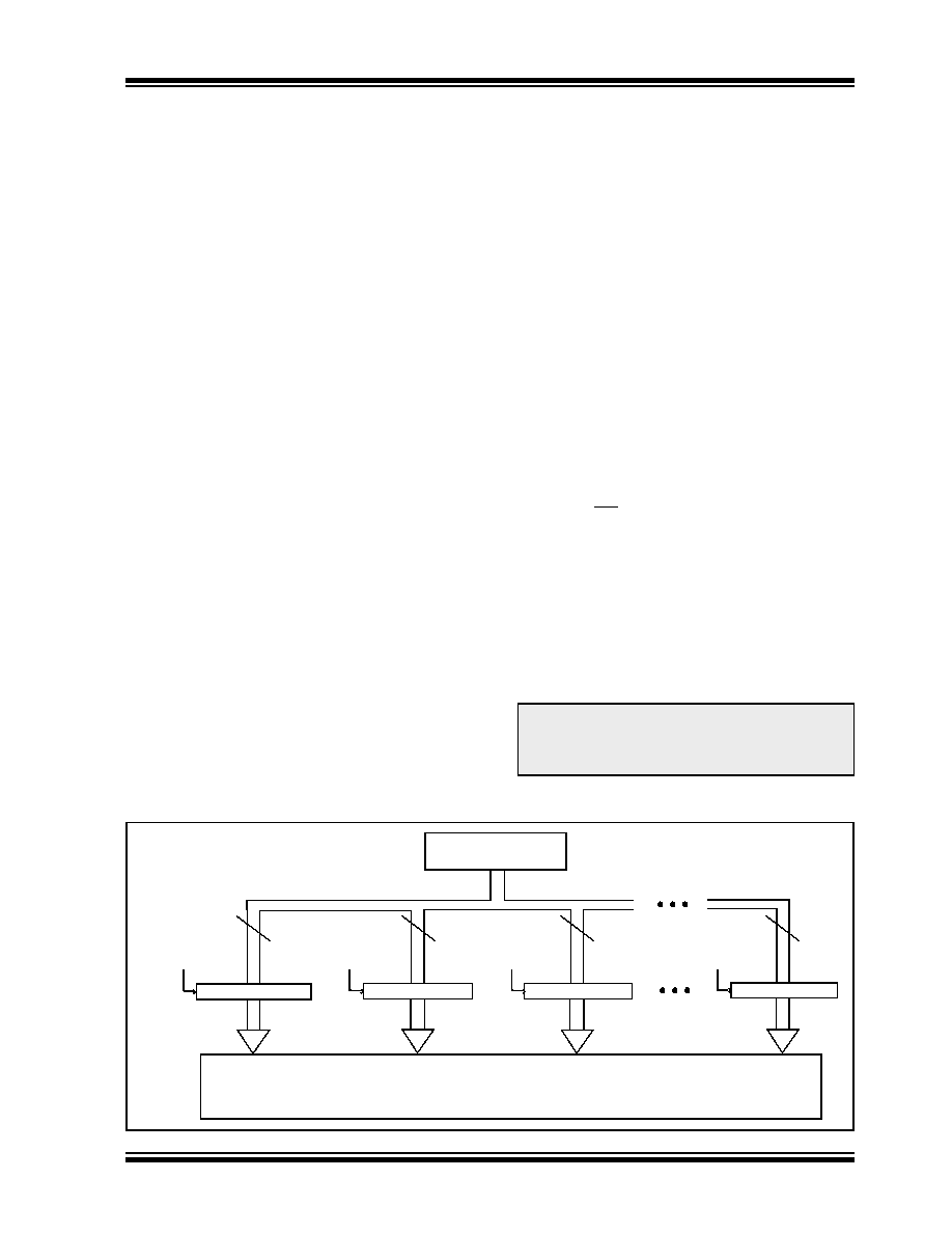
FIGURE 6-5:
TABLE WRITES TO FLASH PROGRAM MEMORY
Note:
Before setting the WR bit, the Table
Pointer address needs to be within the
intended address range of the 8 bytes in
the holding registers.
Holding Register
TABLAT
Holding Register
TBLPTR = xxxxx7
Holding Register
TBLPTR = xxxxx1
Holding Register
TBLPTR = xxxxx0
8
Write Register
TBLPTR = xxxxx2
Program Memory
相关PDF资料 |
PDF描述 |
|---|---|
| PIC16LC77-04I/PQ | IC MCU OTP 8KX14 A/D PWM 44-MQFP |
| GRM31MR61C685KA12L | CAP CER 6.8UF 16V 10% X5R 1206 |
| RPER72A333K2P1C03B | CAP CER 0.033UF 100V 10% RADIAL |
| RPER72A333K2K1C03B | CAP CER 0.033UF 100V 10% RADIAL |
| PIC16C57-HSI/SO | IC MCU OTP 2KX12 28SOIC |
相关代理商/技术参数 |
参数描述 |
|---|---|
| PIC18F45J10-E/ML | 功能描述:8位微控制器 -MCU 32 KB Flash 1 KB RAM RoHS:否 制造商:Silicon Labs 核心:8051 处理器系列:C8051F39x 数据总线宽度:8 bit 最大时钟频率:50 MHz 程序存储器大小:16 KB 数据 RAM 大小:1 KB 片上 ADC:Yes 工作电源电压:1.8 V to 3.6 V 工作温度范围:- 40 C to + 105 C 封装 / 箱体:QFN-20 安装风格:SMD/SMT |
| PIC18F45J10-E/P | 功能描述:8位微控制器 -MCU 32 KB Flash 1 KB RAM RoHS:否 制造商:Silicon Labs 核心:8051 处理器系列:C8051F39x 数据总线宽度:8 bit 最大时钟频率:50 MHz 程序存储器大小:16 KB 数据 RAM 大小:1 KB 片上 ADC:Yes 工作电源电压:1.8 V to 3.6 V 工作温度范围:- 40 C to + 105 C 封装 / 箱体:QFN-20 安装风格:SMD/SMT |
| PIC18F45J10-E/PT | 功能描述:8位微控制器 -MCU 32 KB Flash 1 KB RAM RoHS:否 制造商:Silicon Labs 核心:8051 处理器系列:C8051F39x 数据总线宽度:8 bit 最大时钟频率:50 MHz 程序存储器大小:16 KB 数据 RAM 大小:1 KB 片上 ADC:Yes 工作电源电压:1.8 V to 3.6 V 工作温度范围:- 40 C to + 105 C 封装 / 箱体:QFN-20 安装风格:SMD/SMT |
| PIC18F45J10-I/ML | 功能描述:8位微控制器 -MCU 32 KB FL 1024 RAM RoHS:否 制造商:Silicon Labs 核心:8051 处理器系列:C8051F39x 数据总线宽度:8 bit 最大时钟频率:50 MHz 程序存储器大小:16 KB 数据 RAM 大小:1 KB 片上 ADC:Yes 工作电源电压:1.8 V to 3.6 V 工作温度范围:- 40 C to + 105 C 封装 / 箱体:QFN-20 安装风格:SMD/SMT |
| PIC18F45J10-I/P | 功能描述:8位微控制器 -MCU 32 KB FL 1 KB RAM RoHS:否 制造商:Silicon Labs 核心:8051 处理器系列:C8051F39x 数据总线宽度:8 bit 最大时钟频率:50 MHz 程序存储器大小:16 KB 数据 RAM 大小:1 KB 片上 ADC:Yes 工作电源电压:1.8 V to 3.6 V 工作温度范围:- 40 C to + 105 C 封装 / 箱体:QFN-20 安装风格:SMD/SMT |
发布紧急采购,3分钟左右您将得到回复。