- 您现在的位置:买卖IC网 > PDF目录11344 > PIC18F4610-E/P (Microchip Technology)IC MCU FLASH 32KX16 40DIP PDF资料下载
参数资料
| 型号: | PIC18F4610-E/P |
| 厂商: | Microchip Technology |
| 文件页数: | 199/234页 |
| 文件大小: | 0K |
| 描述: | IC MCU FLASH 32KX16 40DIP |
| 产品培训模块: | Asynchronous Stimulus |
| 标准包装: | 10 |
| 系列: | PIC® 18F |
| 核心处理器: | PIC |
| 芯体尺寸: | 8-位 |
| 速度: | 25MHz |
| 连通性: | I²C,SPI,UART/USART |
| 外围设备: | 欠压检测/复位,HLVD,POR,PWM,WDT |
| 输入/输出数: | 36 |
| 程序存储器容量: | 64KB(32K x 16) |
| 程序存储器类型: | 闪存 |
| RAM 容量: | 3.8K x 8 |
| 电压 - 电源 (Vcc/Vdd): | 4.2 V ~ 5.5 V |
| 数据转换器: | A/D 13x10b |
| 振荡器型: | 内部 |
| 工作温度: | -40°C ~ 125°C |
| 封装/外壳: | 40-DIP(0.600",15.24mm) |
| 包装: | 管件 |
| 配用: | DVA18XP400-ND - DEVICE ADAPTER 18F4220 PDIP 40LD ACICE0206-ND - ADAPTER MPLABICE 40P 600 MIL |
第1页第2页第3页第4页第5页第6页第7页第8页第9页第10页第11页第12页第13页第14页第15页第16页第17页第18页第19页第20页第21页第22页第23页第24页第25页第26页第27页第28页第29页第30页第31页第32页第33页第34页第35页第36页第37页第38页第39页第40页第41页第42页第43页第44页第45页第46页第47页第48页第49页第50页第51页第52页第53页第54页第55页第56页第57页第58页第59页第60页第61页第62页第63页第64页第65页第66页第67页第68页第69页第70页第71页第72页第73页第74页第75页第76页第77页第78页第79页第80页第81页第82页第83页第84页第85页第86页第87页第88页第89页第90页第91页第92页第93页第94页第95页第96页第97页第98页第99页第100页第101页第102页第103页第104页第105页第106页第107页第108页第109页第110页第111页第112页第113页第114页第115页第116页第117页第118页第119页第120页第121页第122页第123页第124页第125页第126页第127页第128页第129页第130页第131页第132页第133页第134页第135页第136页第137页第138页第139页第140页第141页第142页第143页第144页第145页第146页第147页第148页第149页第150页第151页第152页第153页第154页第155页第156页第157页第158页第159页第160页第161页第162页第163页第164页第165页第166页第167页第168页第169页第170页第171页第172页第173页第174页第175页第176页第177页第178页第179页第180页第181页第182页第183页第184页第185页第186页第187页第188页第189页第190页第191页第192页第193页第194页第195页第196页第197页第198页当前第199页第200页第201页第202页第203页第204页第205页第206页第207页第208页第209页第210页第211页第212页第213页第214页第215页第216页第217页第218页第219页第220页第221页第222页第223页第224页第225页第226页第227页第228页第229页第230页第231页第232页第233页第234页
2009 Microchip Technology Inc.
DS39636D-page 69
PIC18F2X1X/4X1X
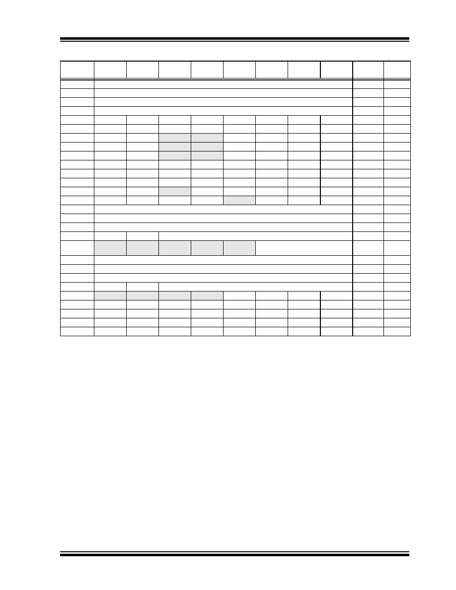
SPBRGH
EUSART Baud Rate Generator Register High Byte
0000 0000
SPBRG
EUSART Baud Rate Generator Register Low Byte
0000 0000
RCREG
EUSART Receive Register
0000 0000
TXREG
EUSART Transmit Register
0000 0000
TXSTA
CSRC
TX9
TXEN
SYNC
SENDB
BRGH
TRMT
TX9D
0000 0010
RCSTA
SPEN
RX9
SREN
CREN
ADDEN
FERR
OERR
RX9D
0000 000x
IPR2
OSCFIP
CMIP
—
BCLIP
HLVDIP
TMR3IP
CCP2IP
11-- 1111
PIR2
OSCFIF
CMIF
—
BCLIF
HLVDIF
TMR3IF
CCP2IF
00-- 0000
PIE2
OSCFIE
CMIE
—
BCLIE
HLVDIE
TMR3IE
CCP2IE
00-- 0000
IPR1
PSPIP(2)
ADIP
RCIP
TXIP
SSPIP
CCP1IP
TMR2IP
TMR1IP
1111 1111
PIR1
PSPIF(2)
ADIF
RCIF
TXIF
SSPIF
CCP1IF
TMR2IF
TMR1IF
0000 0000
PIE1
PSPIE(2)
ADIE
RCIE
TXIE
SSPIE
CCP1IE
TMR2IE
TMR1IE
0000 0000
OSCTUNE
INTSRC
PLLEN(3)
—
TUN4
TUN3
TUN2
TUN1
TUN0
0q-0 0000
TRISE(2)
IBF
OBF
IBOV
PSPMODE
—
TRISE2
TRISE1
TRISE0
0000 -111
TRISD(2)
PORTD Data Direction Control Register
1111 1111
TRISC
PORTC Data Direction Control Register
1111 1111
TRISB
PORTB Data Direction Control Register
1111 1111
TRISA
TRISA7(5)
TRISA6(5)
Data Direction Control Register for PORTA
1111 1111
LATE(2)
—
PORTE Data Latch Register
(Read and Write to Data Latch)
---- -xxx
LATD(2)
PORTD Data Latch Register (Read and Write to Data Latch)
xxxx xxxx
LATC
PORTC Data Latch Register (Read and Write to Data Latch)
xxxx xxxx
LATB
PORTB Data Latch Register (Read and Write to Data Latch)
xxxx xxxx
LATA
LATA7(6)
LATA6(6)
PORTA Data Latch Register (Read and Write to Data Latch)
xxxx xxxx
PORTE
—
—RE3(4)
RE2(2)
RE1(2)
RE0(2)
---- xxxx
PORTD(2)
RD7
RD6
RD5
RD4
RD3
RD2
RD1
RD0
xxxx xxxx
PORTC
RC7
RC6
RC5
RC4
RC3
RC2
RC1
RC0
xxxx xxxx
PORTB
RB7
RB6
RB5
RB4
RB3
RB2
RB1
RB0
xxxx xxxx
PORTA
RA7(5)
RA6(5)
RA5
RA4
RA3
RA2
RA1
RA0
xx0x 0000
TABLE 5-2:
REGISTER FILE SUMMARY (PIC18F2X1X/4X1X) (CONTINUED)
File Name
Bit 7
Bit 6
Bit 5
Bit 4
Bit 3
Bit 2
Bit 1
Bit 0
Value on
POR, BOR
Details
on page:
Legend:
x = unknown, u = unchanged, — = unimplemented, q = value depends on condition
Note
1:
The SBOREN bit is only available when the BOREN1:BOREN0 Configuration bits = 01; otherwise, it is disabled and reads as ‘0’. See
Section 4.4 “Brown-out Reset (BOR)”.
2:
These registers and/or bits are not implemented on 28-pin devices and are read as
‘0’. Reset values are shown for 40/44-pin devices;
individual unimplemented bits should be interpreted as ‘-’.
3:
The PLLEN bit is only available in specific oscillator configuration; otherwise it is disabled and reads as
‘0’. See Section 2.6.4 “PLL in
INTOSC Modes”.
4:
The RE3 bit is only available when Master Clear Reset is disabled (MCLRE Configuration bit = 0). Otherwise, RE3 reads as ‘0’. This bit is
read-only.
5:
RA6/RA7 and their associated latch and direction bits are individually configured as port pins based on various primary oscillator modes.
When disabled, these bits read as ‘0’.
6:
Bit 7 and bit 6 are cleared by user software or by a POR.
相关PDF资料 |
PDF描述 |
|---|---|
| DSPIC33FJ32GP202-E/SP | IC DSPIC MCU/DSP 32K 28DIP |
| VE-21J-IX-F1 | CONVERTER MOD DC/DC 36V 75W |
| VI-21J-IX-F4 | CONVERTER MOD DC/DC 36V 75W |
| PIC16C64A-10/P | IC MCU OTP 2KX14 PWM 40DIP |
| PIC18LF2580-I/SP | IC PIC MCU FLASH 16KX16 28-DIP |
相关代理商/技术参数 |
参数描述 |
|---|---|
| PIC18F4610-I/ML | 功能描述:8位微控制器 -MCU 64KB 3968 RAM 36 I/O RoHS:否 制造商:Silicon Labs 核心:8051 处理器系列:C8051F39x 数据总线宽度:8 bit 最大时钟频率:50 MHz 程序存储器大小:16 KB 数据 RAM 大小:1 KB 片上 ADC:Yes 工作电源电压:1.8 V to 3.6 V 工作温度范围:- 40 C to + 105 C 封装 / 箱体:QFN-20 安装风格:SMD/SMT |
| PIC18F4610-I/P | 功能描述:8位微控制器 -MCU 64KB 3968 RAM 36 I/O RoHS:否 制造商:Silicon Labs 核心:8051 处理器系列:C8051F39x 数据总线宽度:8 bit 最大时钟频率:50 MHz 程序存储器大小:16 KB 数据 RAM 大小:1 KB 片上 ADC:Yes 工作电源电压:1.8 V to 3.6 V 工作温度范围:- 40 C to + 105 C 封装 / 箱体:QFN-20 安装风格:SMD/SMT |
| PIC18F4610-I/P | 制造商:Microchip Technology Inc 功能描述:8-Bit Microcontroller IC |
| PIC18F4610-I/PT | 功能描述:8位微控制器 -MCU 64KB 3968 RAM 36 I/O RoHS:否 制造商:Silicon Labs 核心:8051 处理器系列:C8051F39x 数据总线宽度:8 bit 最大时钟频率:50 MHz 程序存储器大小:16 KB 数据 RAM 大小:1 KB 片上 ADC:Yes 工作电源电压:1.8 V to 3.6 V 工作温度范围:- 40 C to + 105 C 封装 / 箱体:QFN-20 安装风格:SMD/SMT |
| PIC18F4610T-I/ML | 功能描述:8位微控制器 -MCU 64KB 3968 RAM 36 I/O RoHS:否 制造商:Silicon Labs 核心:8051 处理器系列:C8051F39x 数据总线宽度:8 bit 最大时钟频率:50 MHz 程序存储器大小:16 KB 数据 RAM 大小:1 KB 片上 ADC:Yes 工作电源电压:1.8 V to 3.6 V 工作温度范围:- 40 C to + 105 C 封装 / 箱体:QFN-20 安装风格:SMD/SMT |
发布紧急采购,3分钟左右您将得到回复。