- 您现在的位置:买卖IC网 > PDF目录11344 > PIC18F4610-E/P (Microchip Technology)IC MCU FLASH 32KX16 40DIP PDF资料下载
参数资料
| 型号: | PIC18F4610-E/P |
| 厂商: | Microchip Technology |
| 文件页数: | 51/234页 |
| 文件大小: | 0K |
| 描述: | IC MCU FLASH 32KX16 40DIP |
| 产品培训模块: | Asynchronous Stimulus |
| 标准包装: | 10 |
| 系列: | PIC® 18F |
| 核心处理器: | PIC |
| 芯体尺寸: | 8-位 |
| 速度: | 25MHz |
| 连通性: | I²C,SPI,UART/USART |
| 外围设备: | 欠压检测/复位,HLVD,POR,PWM,WDT |
| 输入/输出数: | 36 |
| 程序存储器容量: | 64KB(32K x 16) |
| 程序存储器类型: | 闪存 |
| RAM 容量: | 3.8K x 8 |
| 电压 - 电源 (Vcc/Vdd): | 4.2 V ~ 5.5 V |
| 数据转换器: | A/D 13x10b |
| 振荡器型: | 内部 |
| 工作温度: | -40°C ~ 125°C |
| 封装/外壳: | 40-DIP(0.600",15.24mm) |
| 包装: | 管件 |
| 配用: | DVA18XP400-ND - DEVICE ADAPTER 18F4220 PDIP 40LD ACICE0206-ND - ADAPTER MPLABICE 40P 600 MIL |
第1页第2页第3页第4页第5页第6页第7页第8页第9页第10页第11页第12页第13页第14页第15页第16页第17页第18页第19页第20页第21页第22页第23页第24页第25页第26页第27页第28页第29页第30页第31页第32页第33页第34页第35页第36页第37页第38页第39页第40页第41页第42页第43页第44页第45页第46页第47页第48页第49页第50页当前第51页第52页第53页第54页第55页第56页第57页第58页第59页第60页第61页第62页第63页第64页第65页第66页第67页第68页第69页第70页第71页第72页第73页第74页第75页第76页第77页第78页第79页第80页第81页第82页第83页第84页第85页第86页第87页第88页第89页第90页第91页第92页第93页第94页第95页第96页第97页第98页第99页第100页第101页第102页第103页第104页第105页第106页第107页第108页第109页第110页第111页第112页第113页第114页第115页第116页第117页第118页第119页第120页第121页第122页第123页第124页第125页第126页第127页第128页第129页第130页第131页第132页第133页第134页第135页第136页第137页第138页第139页第140页第141页第142页第143页第144页第145页第146页第147页第148页第149页第150页第151页第152页第153页第154页第155页第156页第157页第158页第159页第160页第161页第162页第163页第164页第165页第166页第167页第168页第169页第170页第171页第172页第173页第174页第175页第176页第177页第178页第179页第180页第181页第182页第183页第184页第185页第186页第187页第188页第189页第190页第191页第192页第193页第194页第195页第196页第197页第198页第199页第200页第201页第202页第203页第204页第205页第206页第207页第208页第209页第210页第211页第212页第213页第214页第215页第216页第217页第218页第219页第220页第221页第222页第223页第224页第225页第226页第227页第228页第229页第230页第231页第232页第233页第234页
PIC18F2X1X/4X1X
DS39636D-page 146
2009 Microchip Technology Inc.
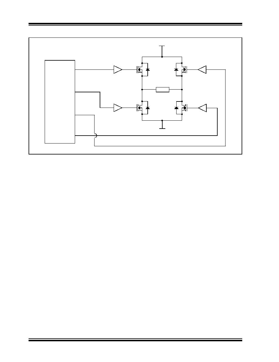
FIGURE 15-7:
EXAMPLE OF FULL-BRIDGE APPLICATION
15.4.5.1
Direction Change in Full-Bridge Mode
In the Full-Bridge Output mode, the P1M1 bit in the
CCP1CON register allows user to control the forward/
reverse direction. When the application firmware
changes this direction control bit, the module will
assume the new direction on the next PWM cycle.
Just before the end of the current PWM period, the
modulated outputs (P1B and P1D) are placed in their
inactive state, while the unmodulated outputs (P1A and
P1C) are switched to drive in the opposite direction.
This occurs in a time interval of 4 TOSC * (Timer2
Prescale Value) before the next PWM period begins.
The Timer2 prescaler will be either 1, 4 or 16, depend-
ing on the value of the T2CKPS bit (T2CON<1:0>).
During the interval from the switch of the unmodulated
outputs to the beginning of the next period, the
modulated outputs (P1B and P1D) remain inactive.
This relationship is shown in Figure 15-8.
Note that in the Full-Bridge Output mode, the CCP1
module does not provide any dead-band delay. In
general, since only one output is modulated at all times,
dead-band delay is not required. However, there is a
situation where a dead-band delay might be required.
This situation occurs when both of the following
conditions are true:
1.
The direction of the PWM output changes when
the duty cycle of the output is at or near 100%.
2.
The turn-off time of the power switch, including
the power device and driver circuit, is greater
than the turn-on time.
Figure 15-9 shows an example where the PWM
direction changes from forward to reverse at a near
100% duty cycle. At time t1, the outputs P1A and P1D
become inactive, while output P1C becomes active. In
this example, since the turn-off time of the power
devices is longer than the turn-on time, a shoot-through
current may flow through power devices, QC and QD
(see Figure 15-7), for the duration of ‘t’. The same
phenomenon will occur to power devices, QA and QB,
for PWM direction change from reverse to forward.
If changing PWM direction at high duty cycle is required
for an application, one of the following requirements
must be met:
1.
Reduce PWM for a PWM period before
changing directions.
2.
Use switch drivers that can drive the switches off
faster than they can drive them on.
Other options to prevent shoot-through current may
exist.
P1A
P1C
FET
Driver
FET
Driver
V+
V-
Load
FET
Driver
FET
Driver
P1B
P1D
QA
QB
QD
QC
PIC18F4X1X
相关PDF资料 |
PDF描述 |
|---|---|
| DSPIC33FJ32GP202-E/SP | IC DSPIC MCU/DSP 32K 28DIP |
| VE-21J-IX-F1 | CONVERTER MOD DC/DC 36V 75W |
| VI-21J-IX-F4 | CONVERTER MOD DC/DC 36V 75W |
| PIC16C64A-10/P | IC MCU OTP 2KX14 PWM 40DIP |
| PIC18LF2580-I/SP | IC PIC MCU FLASH 16KX16 28-DIP |
相关代理商/技术参数 |
参数描述 |
|---|---|
| PIC18F4610-I/ML | 功能描述:8位微控制器 -MCU 64KB 3968 RAM 36 I/O RoHS:否 制造商:Silicon Labs 核心:8051 处理器系列:C8051F39x 数据总线宽度:8 bit 最大时钟频率:50 MHz 程序存储器大小:16 KB 数据 RAM 大小:1 KB 片上 ADC:Yes 工作电源电压:1.8 V to 3.6 V 工作温度范围:- 40 C to + 105 C 封装 / 箱体:QFN-20 安装风格:SMD/SMT |
| PIC18F4610-I/P | 功能描述:8位微控制器 -MCU 64KB 3968 RAM 36 I/O RoHS:否 制造商:Silicon Labs 核心:8051 处理器系列:C8051F39x 数据总线宽度:8 bit 最大时钟频率:50 MHz 程序存储器大小:16 KB 数据 RAM 大小:1 KB 片上 ADC:Yes 工作电源电压:1.8 V to 3.6 V 工作温度范围:- 40 C to + 105 C 封装 / 箱体:QFN-20 安装风格:SMD/SMT |
| PIC18F4610-I/P | 制造商:Microchip Technology Inc 功能描述:8-Bit Microcontroller IC |
| PIC18F4610-I/PT | 功能描述:8位微控制器 -MCU 64KB 3968 RAM 36 I/O RoHS:否 制造商:Silicon Labs 核心:8051 处理器系列:C8051F39x 数据总线宽度:8 bit 最大时钟频率:50 MHz 程序存储器大小:16 KB 数据 RAM 大小:1 KB 片上 ADC:Yes 工作电源电压:1.8 V to 3.6 V 工作温度范围:- 40 C to + 105 C 封装 / 箱体:QFN-20 安装风格:SMD/SMT |
| PIC18F4610T-I/ML | 功能描述:8位微控制器 -MCU 64KB 3968 RAM 36 I/O RoHS:否 制造商:Silicon Labs 核心:8051 处理器系列:C8051F39x 数据总线宽度:8 bit 最大时钟频率:50 MHz 程序存储器大小:16 KB 数据 RAM 大小:1 KB 片上 ADC:Yes 工作电源电压:1.8 V to 3.6 V 工作温度范围:- 40 C to + 105 C 封装 / 箱体:QFN-20 安装风格:SMD/SMT |
发布紧急采购,3分钟左右您将得到回复。