- 您现在的位置:买卖IC网 > PDF目录11248 > PIC18F6620-E/PT (Microchip Technology)IC PIC MCU FLASH 32KX16 64TQFP PDF资料下载
参数资料
| 型号: | PIC18F6620-E/PT |
| 厂商: | Microchip Technology |
| 文件页数: | 84/165页 |
| 文件大小: | 0K |
| 描述: | IC PIC MCU FLASH 32KX16 64TQFP |
| 产品培训模块: | Asynchronous Stimulus |
| 标准包装: | 160 |
| 系列: | PIC® 18F |
| 核心处理器: | PIC |
| 芯体尺寸: | 8-位 |
| 速度: | 25MHz |
| 连通性: | I²C,SPI,UART/USART |
| 外围设备: | 欠压检测/复位,LVD,POR,PWM,WDT |
| 输入/输出数: | 52 |
| 程序存储器容量: | 64KB(32K x 16) |
| 程序存储器类型: | 闪存 |
| EEPROM 大小: | 1K x 8 |
| RAM 容量: | 3.75K x 8 |
| 电压 - 电源 (Vcc/Vdd): | 4.2 V ~ 5.5 V |
| 数据转换器: | A/D 12x10b |
| 振荡器型: | 外部 |
| 工作温度: | -40°C ~ 125°C |
| 封装/外壳: | 64-TQFP |
| 包装: | 托盘 |
第1页第2页第3页第4页第5页第6页第7页第8页第9页第10页第11页第12页第13页第14页第15页第16页第17页第18页第19页第20页第21页第22页第23页第24页第25页第26页第27页第28页第29页第30页第31页第32页第33页第34页第35页第36页第37页第38页第39页第40页第41页第42页第43页第44页第45页第46页第47页第48页第49页第50页第51页第52页第53页第54页第55页第56页第57页第58页第59页第60页第61页第62页第63页第64页第65页第66页第67页第68页第69页第70页第71页第72页第73页第74页第75页第76页第77页第78页第79页第80页第81页第82页第83页当前第84页第85页第86页第87页第88页第89页第90页第91页第92页第93页第94页第95页第96页第97页第98页第99页第100页第101页第102页第103页第104页第105页第106页第107页第108页第109页第110页第111页第112页第113页第114页第115页第116页第117页第118页第119页第120页第121页第122页第123页第124页第125页第126页第127页第128页第129页第130页第131页第132页第133页第134页第135页第136页第137页第138页第139页第140页第141页第142页第143页第144页第145页第146页第147页第148页第149页第150页第151页第152页第153页第154页第155页第156页第157页第158页第159页第160页第161页第162页第163页第164页第165页
2004 Microchip Technology Inc.
DS39609B-page 23
PIC18F6520/8520/6620/8620/6720/8720
2.4
External Clock Input
The EC and ECIO Oscillator modes require an external
clock source to be connected to the OSC1 pin. The
feedback device between OSC1 and OSC2 is turned
off in these modes to save current. There is a maximum
1.5
s start-up required after a Power-on Reset, or
wake-up from Sleep mode.
In the EC Oscillator mode, the oscillator frequency
divided by 4 is available on the OSC2 pin. This signal
may be used for test purposes or to synchronize other
logic. Figure 2-4 shows the pin connections for the EC
Oscillator mode.
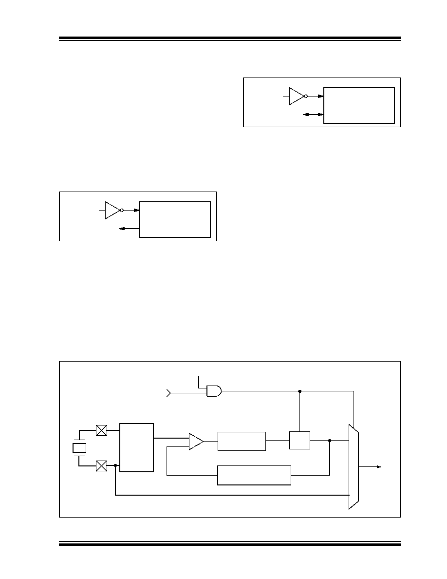
FIGURE 2-4:
EXTERNAL CLOCK INPUT
OPERATION
(EC CONFIGURATION)
The ECIO Oscillator mode functions like the EC mode,
except that the OSC2 pin becomes an additional gen-
eral purpose I/O pin. The I/O pin becomes bit 6 of
PORTA (RA6). Figure 2-5 shows the pin connections
for the ECIO Oscillator mode.
FIGURE 2-5:
EXTERNAL CLOCK INPUT
OPERATION
(ECIO CONFIGURATION)
2.5
HS/PLL
A Phase Locked Loop circuit (PLL) is provided as a
programmable option for users that want to multiply the
frequency of the incoming crystal oscillator signal by 4.
For an input clock frequency of 10 MHz, the internal
clock frequency will be multiplied to 40 MHz. This is
useful for customers who are concerned with EMI due
to high-frequency crystals.
The PLL is one of the modes of the FOSC<2:0> config-
uration bits. The oscillator mode is specified during
device programming.
The PLL can only be enabled when the oscillator con-
figuration bits are programmed for HS mode. If they are
programmed for any other mode, the PLL is not
enabled and the system clock will come directly from
OSC1. Also, PLL operation cannot be changed “on-
the-fly”. To enable or disable it, the controller must
either cycle through a Power-on Reset, or switch the
clock source from the main oscillator to the Timer1
oscillator and back again. See Section 2.6 “Oscillator
Switching Feature” for details on oscillator switching.
A PLL lock timer is used to ensure that the PLL has
locked before device execution starts. The PLL lock
timer has a time-out that is called TPLL.
FIGURE 2-6:
PLL BLOCK DIAGRAM
OSC1
OSC2
FOSC/4
Clock from
Ext. System
PIC18FXX20
OSC1
I/O (OSC2)
RA6
Clock from
Ext. System
PIC18FXX20
MUX
VCO
Loop
Filter
Divide by 4
Crystal
Osc
OSC2
OSC1
PLL Enable
FIN
FOUT
SYSCLK
Phase
Comparator
(from Configuration
HS Osc
bit Register)
相关PDF资料 |
PDF描述 |
|---|---|
| ADG721BRM | IC SWITCH DUAL SPST 8MSOP |
| PIC17C44-33/PT | IC MCU OTP 8KX16 PWM 44TQFP |
| PIC17C44-25/PT | IC MCU OTP 8KX16 PWM 44TQFP |
| ADG713BRU-REEL7 | IC SWITCH QUAD SPST 16TSSOP |
| ADG712BR-REEL7 | IC SWITCH QUAD SPST 16SOIC |
相关代理商/技术参数 |
参数描述 |
|---|---|
| PIC18F6620-I/PT | 功能描述:8位微控制器 -MCU 64KB 3840 RAM 52I/O RoHS:否 制造商:Silicon Labs 核心:8051 处理器系列:C8051F39x 数据总线宽度:8 bit 最大时钟频率:50 MHz 程序存储器大小:16 KB 数据 RAM 大小:1 KB 片上 ADC:Yes 工作电源电压:1.8 V to 3.6 V 工作温度范围:- 40 C to + 105 C 封装 / 箱体:QFN-20 安装风格:SMD/SMT |
| PIC18F6620-I/PT | 制造商:Microchip Technology Inc 功能描述:IC 8BIT FLASH MCU 18F6620 TQFP64 |
| PIC18F6620-I/PTC01 | 制造商:Microchip Technology 功能描述:MCU 8-Bit PIC18 PIC RISC 64KB Flash 5V 64-Pin TQFP Tray |
| PIC18F6620T-I/PT | 功能描述:8位微控制器 -MCU 64KB 3840 RAM 52I/O RoHS:否 制造商:Silicon Labs 核心:8051 处理器系列:C8051F39x 数据总线宽度:8 bit 最大时钟频率:50 MHz 程序存储器大小:16 KB 数据 RAM 大小:1 KB 片上 ADC:Yes 工作电源电压:1.8 V to 3.6 V 工作温度范围:- 40 C to + 105 C 封装 / 箱体:QFN-20 安装风格:SMD/SMT |
| PIC18F6621-E/PT | 功能描述:8位微控制器 -MCU 64KB 3840 RAM 52I/O RoHS:否 制造商:Silicon Labs 核心:8051 处理器系列:C8051F39x 数据总线宽度:8 bit 最大时钟频率:50 MHz 程序存储器大小:16 KB 数据 RAM 大小:1 KB 片上 ADC:Yes 工作电源电压:1.8 V to 3.6 V 工作温度范围:- 40 C to + 105 C 封装 / 箱体:QFN-20 安装风格:SMD/SMT |
发布紧急采购,3分钟左右您将得到回复。