- 您现在的位置:买卖IC网 > PDF目录3869 > PIC18F66J93-I/PT (Microchip Technology)IC PIC MCU FLASH 64KX4 64-TQFP PDF资料下载
参数资料
| 型号: | PIC18F66J93-I/PT |
| 厂商: | Microchip Technology |
| 文件页数: | 31/54页 |
| 文件大小: | 0K |
| 描述: | IC PIC MCU FLASH 64KX4 64-TQFP |
| 产品培训模块: | PIC18 J Series MCU Overview |
| 标准包装: | 160 |
| 系列: | PIC® 18F |
| 核心处理器: | PIC |
| 芯体尺寸: | 8-位 |
| 速度: | 48MHz |
| 连通性: | I²C,LIN,SPI,UART/USART |
| 外围设备: | 欠压检测/复位,LCD,LVD,POR,PWM,WDT |
| 输入/输出数: | 51 |
| 程序存储器容量: | 64KB(32K x 16) |
| 程序存储器类型: | 闪存 |
| RAM 容量: | 3923 x 8 |
| 电压 - 电源 (Vcc/Vdd): | 2 V ~ 3.6 V |
| 数据转换器: | A/D 12x12b |
| 振荡器型: | 内部 |
| 工作温度: | -40°C ~ 85°C |
| 封装/外壳: | 64-TQFP |
| 包装: | 托盘 |
第1页第2页第3页第4页第5页第6页第7页第8页第9页第10页第11页第12页第13页第14页第15页第16页第17页第18页第19页第20页第21页第22页第23页第24页第25页第26页第27页第28页第29页第30页当前第31页第32页第33页第34页第35页第36页第37页第38页第39页第40页第41页第42页第43页第44页第45页第46页第47页第48页第49页第50页第51页第52页第53页第54页
2009 Microchip Technology Inc.
Preliminary
DS39948A-page 35
PIC18F87J93 FAMILY
2.7
A/D Converter Calibration
The A/D converter in the PIC18F87J93 family of
devices includes a self-calibration feature which com-
pensates for any offset generated within the module.
The calibration process is automated and is initiated by
setting the ADCAL bit (ADCON0<7>). The next time
the GO/DONE bit is set, the module will perform a
“dummy” conversion (which means it is reading none of
the input channels) and store the resulting value
internally to compensate for offset. Thus, subsequent
offsets will be compensated.
The calibration process assumes that the device is in a
relatively steady-state operating condition. If A/D
calibration is used, it should be performed after each
device Reset or if there are other major changes in
operating conditions.
2.8
Operation in Power-Managed
Modes
The selection of the automatic acquisition time and A/D
conversion clock is determined in part by the clock
source and frequency while in a power-managed mode.
If the A/D is expected to operate while the device is in
a
power-managed
mode,
the
ACQT<2:0>
and
ADCS<2:0> bits in ADCON2 should be updated in
accordance with the power-managed mode clock that
will be used. After the power-managed mode is entered
(either of the power-managed Run modes), an A/D
acquisition or conversion may be started. Once an
acquisition or conversion is started, the device should
continue to be clocked by the same power-managed
mode clock source until the conversion has been
completed. If desired, the device may be placed into
the corresponding power-managed Idle mode during
the conversion.
If the power-managed mode clock frequency is less
than 1 MHz, the A/D RC clock source should be
selected.
Operation in Sleep mode requires the A/D RC clock to
be selected. If bits, ACQT<2:0>, are set to ‘000’ and a
conversion is started, the conversion will be delayed
one instruction cycle to allow execution of the SLEEP
instruction and entry to Sleep mode. The IDLEN and
SCSx bits in the OSCCON register must have already
been cleared prior to starting the conversion.
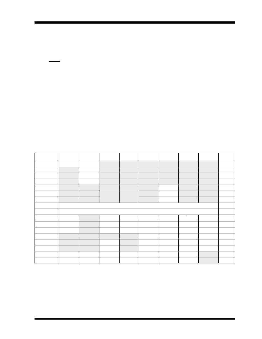
TABLE 2-2:
SUMMARY OF A/D REGISTERS
Name
Bit 7
Bit 6
Bit 5
Bit 4
Bit 3
Bit 2
Bit 1
Bit 0
Notes
INTCON
GIE/GIEH PEIE/GIEL
TMR0IE
INT0IE
RBIE
TMR0IF
INT0IF
RBIF
PIR1
—ADIF
RC1IF
TX1IF
SSPIF
—
TMR2IF
TMR1IF
PIE1
—ADIE
RC1IE
TX1IE
SSPIE
—
TMR2IE
TMR1IE
IPR1
—ADIP
RC1IP
TX1IP
SSPIP
—
TMR2IP
TMR1IP
PIR3
—
LCDIF
RC2IF
TX2IF
CTMUIF
CCP2IF
CCP1IF
RTCCIF
PIE3
—
LCDIE
RC2IE
TX2IE
CTMUIE
CCP2IE
CCP1IE
RTCCIE
IPR3
—
LCDIP
RC2IP
TX2IP
CTMUIP
CCP2IP
CCP1IP
RTCCIP
ADRESH
A/D Result Register High Byte
ADRESL
A/D Result Register Low Byte
ADCON0
ADCAL
—
CHS3
CHS2
CHS1
CHS0
GO/DONE
ADON
ADCON1
TRIGSEL
—
VCFG1
VCFG0
PCFG3
PCFG2
PCFG1
PCFG0
ADCON2
ADFM
—
ACQT2
ACQT1
ACQT0
ADCS2
ADCS1
ADCS0
CCP2CON
—
DC2B1
DC2B0
CCP2M3
CCP2M2
CCP2M1
CCP2M0
PORTA
RA7(1)
RA6(1)
RA5
RA4
RA3
RA2
RA1
RA0
TRISA
TRISA7(1) TRISA6(1)
TRISA5
TRISA4
TRISA3
TRISA2
TRISA1
TRISA0
PORTF
RF7
RF6
RF5
RF4
RF3
RF2
RF1
—
TRISF
TRISF5
TRISF4
TRISF5
TRISF4
TRISF3
TRISF2
TRISF1
—
Legend:
— = unimplemented, read as ‘0’. Shaded cells are not used for A/D conversion.
Note 1:
RA<7:6> and their associated latch and direction bits are configured as port pins only when the internal
oscillator is selected as the default clock source (FOSC2 Configuration bit = 0); otherwise, they are
disabled and these bits read as ‘0’.
2:
For these Reset values, see Section 4.0 “Reset” of the “PIC18F87J90 Family Data Sheet” (DS39933).
相关PDF资料 |
PDF描述 |
|---|---|
| DSPIC33FJ64MC510T-I/PT | IC DSPIC MCU/DSP 64K 100TQFP |
| DSPIC33FJ64MC510T-I/PF | IC DSPIC MCU/DSP 64K 100TQFP |
| DSPIC33FJ64GP710T-I/PT | IC DSPIC MCU/DSP 64K 100TQFP |
| DSPIC33FJ64GP710T-I/PF | IC DSPIC MCU/DSP 64K 100TQFP |
| PIC16F1939-I/ML | IC MCU 8BIT FLASH 44QFN |
相关代理商/技术参数 |
参数描述 |
|---|---|
| PIC18F66J93T-I/PT | 功能描述:8位微控制器 -MCU 64pin,4KB RAM,12MIPS SEG LCD, 64KB Flash RoHS:否 制造商:Silicon Labs 核心:8051 处理器系列:C8051F39x 数据总线宽度:8 bit 最大时钟频率:50 MHz 程序存储器大小:16 KB 数据 RAM 大小:1 KB 片上 ADC:Yes 工作电源电压:1.8 V to 3.6 V 工作温度范围:- 40 C to + 105 C 封装 / 箱体:QFN-20 安装风格:SMD/SMT |
| PIC18F66J94-I/MR | 制造商:Microchip Technology Inc 功能描述:64 PINS, 64KB FLASH, 4KB RAM, 16MIPS, NANOWATT XLP, LCD, USB - Rail/Tube 制造商:Microchip Technology Inc 功能描述:IC MCU 8BIT 64KB FLASH 64QFN 制造商:Microchip Technology Inc 功能描述:64 pins, 64KB Flash, 4KB RAM, 16MIPS, nanoWatt XLP, LCD, USB, 64 QFN 9x9x0.9mm T |
| PIC18F66J94-I/PT | 制造商:Microchip Technology Inc 功能描述:64 PINS, 64KB FLASH, 4KB RAM, 16MIPS, NANOWATT XLP, LCD, USB - Trays 制造商:Microchip Technology Inc 功能描述:IC MCU 8BIT 64KB FLASH 64TQFP 制造商:Microchip Technology Inc 功能描述:64 pins, 64KB Flash, 4KB RAM, 16MIPS, nanoWatt XLP, LCD, USB, 64 TQFP 10x10x1mm |
| PIC18F66J94T-I/MR | 制造商:Microchip Technology Inc 功能描述:64 PINS, 64KB FLASH, 4KB RAM, 16MIPS, NANOWATT XLP, LCD, USB - Tape and Reel 制造商:Microchip Technology Inc 功能描述:IC MCU 8BIT 64KB FLASH 64QFN 制造商:Microchip Technology Inc 功能描述:8-bit Microcontrollers - MCU 64 pins 64KB Flash 4KB RAM 16MIPS 制造商:Microchip Technology Inc 功能描述:64 pins, 64KB Flash, 4KB RAM, 16MIPS, nanoWatt XLP, LCD, USB, 64 QFN 9x9x0.9mm T |
| PIC18F66J94T-I/PT | 制造商:Microchip Technology Inc 功能描述:64 PINS, 64KB FLASH, 4KB RAM, 16MIPS, NANOWATT XLP, LCD, USB - Tape and Reel 制造商:Microchip Technology Inc 功能描述:IC MCU 8BIT 64KB FLASH 64TQFP 制造商:Microchip Technology Inc 功能描述:8-bit Microcontrollers - MCU 64 pins, 64KB Flash, 4KB RAM, 16MIPS |
发布紧急采购,3分钟左右您将得到回复。