- 您现在的位置:买卖IC网 > PDF目录11481 > PIC18F67J10T-I/PT (Microchip Technology)IC PIC MCU FLASH 64KX16 64TQFP PDF资料下载
参数资料
| 型号: | PIC18F67J10T-I/PT |
| 厂商: | Microchip Technology |
| 文件页数: | 25/44页 |
| 文件大小: | 0K |
| 描述: | IC PIC MCU FLASH 64KX16 64TQFP |
| 产品培训模块: | Asynchronous Stimulus PIC18 J Series MCU Overview |
| 标准包装: | 1 |
| 系列: | PIC® 18F |
| 核心处理器: | PIC |
| 芯体尺寸: | 8-位 |
| 速度: | 40MHz |
| 连通性: | I²C,SPI,UART/USART |
| 外围设备: | 欠压检测/复位,POR,PWM,WDT |
| 输入/输出数: | 50 |
| 程序存储器容量: | 128KB(64K x 16) |
| 程序存储器类型: | 闪存 |
| RAM 容量: | 3.8K x 8 |
| 电压 - 电源 (Vcc/Vdd): | 2 V ~ 3.6 V |
| 数据转换器: | A/D 11x10b |
| 振荡器型: | 内部 |
| 工作温度: | -40°C ~ 85°C |
| 封装/外壳: | 64-TQFP |
| 包装: | 剪切带 (CT) |
| 配用: | MA180015-ND - MODULE PLUG-IN 18F87J10 FOR HPC AC162062-ND - HEADER INTRFC MPLAB ICD2 64/80P AC164327-ND - MODULE SKT FOR 64TQFP |
| 其它名称: | PIC18F67J10T-I/PTCT |
第1页第2页第3页第4页第5页第6页第7页第8页第9页第10页第11页第12页第13页第14页第15页第16页第17页第18页第19页第20页第21页第22页第23页第24页当前第25页第26页第27页第28页第29页第30页第31页第32页第33页第34页第35页第36页第37页第38页第39页第40页第41页第42页第43页第44页
2009 Microchip Technology Inc.
DS39663F-page 29
PIC18F87J10 FAMILY
2.4
Voltage Regulator Pins (ENVREG
and VCAP/VDDCORE)
The on-chip voltage regulator enable pin, ENVREG,
must always be connected directly to either a supply
voltage or to ground. Tying ENVREG to VDD enables
the regulator, while tying it to ground disables the
regulator. Refer to Section 24.3 “On-Chip Voltage
Regulator” for details on connecting and using the
on-chip regulator.
When the regulator is enabled, a low-ESR (<5)
capacitor is required on the VCAP/VDDCORE pin to
stabilize the voltage regulator output voltage. The
VCAP/VDDCORE pin must not be connected to VDD and
must use a capacitor of 10
μF connected to ground. The
type can be ceramic or tantalum. A suitable example is
the Murata GRM21BF50J106ZE01 (10
μF, 6.3V) or
equivalent. Designers may use Figure 2-3 to evaluate
ESR equivalence of candidate devices.
It is recommended that the trace length not exceed
0.25 inch (6 mm). Refer to Section 27.0 “Electrical
Characteristics” for additional information.
When the regulator is disabled, the VCAP/VDDCORE pin
must be tied to a voltage supply at the VDDCORE level.
Refer to Section 27.0 “Electrical Characteristics” for
information on VDD and VDDCORE.
Note that the “LF” versions of some low pin count
PIC18FJ parts (e.g., the PIC18LF45J10) do not have
the ENVREG pin. These devices are provided with the
voltage regulator permanently disabled; they must
always be provided with a supply voltage on the
VDDCORE pin.
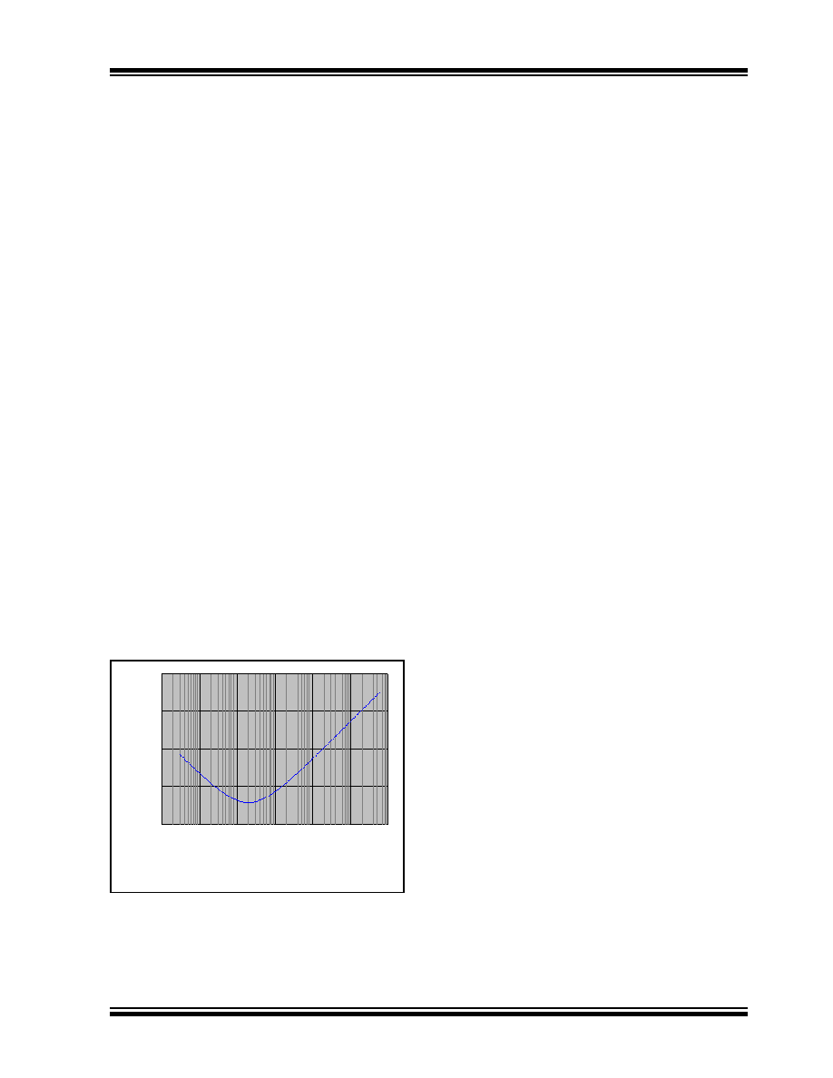
FIGURE 2-3:
FREQUENCY vs. ESR
PERFORMANCE FOR
SUGGESTED VCAP
2.5
ICSP Pins
The PGC and PGD pins are used for In-Circuit Serial
Programming (ICSP) and debugging purposes. It is
recommended to keep the trace length between the
ICSP connector and the ICSP pins on the device as
short as possible. If the ICSP connector is expected to
experience an ESD event, a series resistor is recom-
mended, with the value in the range of a few tens of
ohms, not to exceed 100.
Pull-up resistors, series diodes and capacitors on the
PGC and PGD pins are not recommended as they will
interfere
with
the
programmer/debugger
com-
munications to the device. If such discrete components
are an application requirement, they should be removed
from the circuit during programming and debugging.
Alternatively, refer to the AC/DC characteristics and
timing requirements information in the respective device
Flash programming specification for information on
capacitive loading limits and pin input voltage high (VIH)
and input low (VIL) requirements.
For device emulation, ensure that the “Communication
Channel Select” (i.e., PGC/PGD pins) programmed
into the device matches the physical connections for
the ICSP to the MPLAB ICD 2, MPLAB ICD 3 or
REAL ICE emulator.
For more information on the ICD 2, ICD 3 and REAL ICE
emulator connection requirements, refer to the following
documents that are available on the Microchip web site.
“MPLAB ICD 2 In-Circuit Debugger User’s
Guide” (DS51331)
“Using MPLAB ICD 2” (poster) (DS51265)
“MPLAB ICD 2 Design Advisory” (DS51566)
“Using MPLAB ICD 3” (poster) (DS51765)
“MPLAB ICD 3 Design Advisory” (DS51764)
“MPLAB REAL ICE In-Circuit Emulator User’s
Guide” (DS51616)
“Using MPLAB REAL ICE In-Circuit Emulator”
(poster) (DS51749)
10
1
0.1
0.01
0.001
0.01
0.1
1
10
100
1000 10,000
Frequency (MHz)
ES
R
(
Ω
)
Note:
Data for Murata GRM21BF50J106ZE01 shown.
Measurements at 25°C, 0V DC bias.
相关PDF资料 |
PDF描述 |
|---|---|
| ADG509FBRNZ | IC MULTIPLEXER DUAL 4X1 16SOIC |
| PIC16C770T-I/SS | IC MCU OTP 2KX14 A/D PWM 20SSOP |
| PIC16LC711-04E/P | IC MCU OTP 1KX14 A/D 18DIP |
| VE-BNF-CU-F2 | CONVERTER MOD DC/DC 72V 200W |
| VE-BND-CU-F4 | CONVERTER MOD DC/DC 85V 200W |
相关代理商/技术参数 |
参数描述 |
|---|---|
| PIC18F67J11-I/PT | 功能描述:8位微控制器 -MCU 128KB FL 3936b RAM 10 MIPS 51 I/O RoHS:否 制造商:Silicon Labs 核心:8051 处理器系列:C8051F39x 数据总线宽度:8 bit 最大时钟频率:50 MHz 程序存储器大小:16 KB 数据 RAM 大小:1 KB 片上 ADC:Yes 工作电源电压:1.8 V to 3.6 V 工作温度范围:- 40 C to + 105 C 封装 / 箱体:QFN-20 安装风格:SMD/SMT |
| PIC18F67J11T-I/PT | 功能描述:8位微控制器 -MCU 128KB Flash 3936 bytesRAM 51I/O RoHS:否 制造商:Silicon Labs 核心:8051 处理器系列:C8051F39x 数据总线宽度:8 bit 最大时钟频率:50 MHz 程序存储器大小:16 KB 数据 RAM 大小:1 KB 片上 ADC:Yes 工作电源电压:1.8 V to 3.6 V 工作温度范围:- 40 C to + 105 C 封装 / 箱体:QFN-20 安装风格:SMD/SMT |
| PIC18F67J50-I/PT | 功能描述:8位微控制器 -MCU 128KB FLH 3936Bs RAM USB 2.0 nanoWatt RoHS:否 制造商:Silicon Labs 核心:8051 处理器系列:C8051F39x 数据总线宽度:8 bit 最大时钟频率:50 MHz 程序存储器大小:16 KB 数据 RAM 大小:1 KB 片上 ADC:Yes 工作电源电压:1.8 V to 3.6 V 工作温度范围:- 40 C to + 105 C 封装 / 箱体:QFN-20 安装风格:SMD/SMT |
| PIC18F67J50T-I/PT | 功能描述:8位微控制器 -MCU 128KB FLH 3936Bs RAM USB 2.0 nanoWatt RoHS:否 制造商:Silicon Labs 核心:8051 处理器系列:C8051F39x 数据总线宽度:8 bit 最大时钟频率:50 MHz 程序存储器大小:16 KB 数据 RAM 大小:1 KB 片上 ADC:Yes 工作电源电压:1.8 V to 3.6 V 工作温度范围:- 40 C to + 105 C 封装 / 箱体:QFN-20 安装风格:SMD/SMT |
| PIC18F67J60-I/PT | 功能描述:8位微控制器 -MCU 128KB FL 12KB RAM 10BASE-T RoHS:否 制造商:Silicon Labs 核心:8051 处理器系列:C8051F39x 数据总线宽度:8 bit 最大时钟频率:50 MHz 程序存储器大小:16 KB 数据 RAM 大小:1 KB 片上 ADC:Yes 工作电源电压:1.8 V to 3.6 V 工作温度范围:- 40 C to + 105 C 封装 / 箱体:QFN-20 安装风格:SMD/SMT |
发布紧急采购,3分钟左右您将得到回复。