- 您现在的位置:买卖IC网 > PDF目录11448 > PIC18LF27J53T-I/SO (Microchip Technology)IC MCU 8BIT 128KB FLASH 28SOIC PDF资料下载
参数资料
| 型号: | PIC18LF27J53T-I/SO |
| 厂商: | Microchip Technology |
| 文件页数: | 384/389页 |
| 文件大小: | 0K |
| 描述: | IC MCU 8BIT 128KB FLASH 28SOIC |
| 标准包装: | 1,600 |
| 系列: | PIC® XLP™ 18F |
| 核心处理器: | PIC |
| 芯体尺寸: | 8-位 |
| 速度: | 48MHz |
| 连通性: | I²C,LIN,SPI,UART/USART,USB |
| 外围设备: | 欠压检测/复位,POR,PWM,WDT |
| 输入/输出数: | 22 |
| 程序存储器容量: | 128KB(64K x 16) |
| 程序存储器类型: | 闪存 |
| RAM 容量: | 3.8K x 8 |
| 电压 - 电源 (Vcc/Vdd): | 2 V ~ 2.75 V |
| 数据转换器: | A/D 10x10b/12b |
| 振荡器型: | 内部 |
| 工作温度: | -40°C ~ 85°C |
| 封装/外壳: | 28-SOIC(0.295",7.50mm 宽) |
| 包装: | 带卷 (TR) |
第1页第2页第3页第4页第5页第6页第7页第8页第9页第10页第11页第12页第13页第14页第15页第16页第17页第18页第19页第20页第21页第22页第23页第24页第25页第26页第27页第28页第29页第30页第31页第32页第33页第34页第35页第36页第37页第38页第39页第40页第41页第42页第43页第44页第45页第46页第47页第48页第49页第50页第51页第52页第53页第54页第55页第56页第57页第58页第59页第60页第61页第62页第63页第64页第65页第66页第67页第68页第69页第70页第71页第72页第73页第74页第75页第76页第77页第78页第79页第80页第81页第82页第83页第84页第85页第86页第87页第88页第89页第90页第91页第92页第93页第94页第95页第96页第97页第98页第99页第100页第101页第102页第103页第104页第105页第106页第107页第108页第109页第110页第111页第112页第113页第114页第115页第116页第117页第118页第119页第120页第121页第122页第123页第124页第125页第126页第127页第128页第129页第130页第131页第132页第133页第134页第135页第136页第137页第138页第139页第140页第141页第142页第143页第144页第145页第146页第147页第148页第149页第150页第151页第152页第153页第154页第155页第156页第157页第158页第159页第160页第161页第162页第163页第164页第165页第166页第167页第168页第169页第170页第171页第172页第173页第174页第175页第176页第177页第178页第179页第180页第181页第182页第183页第184页第185页第186页第187页第188页第189页第190页第191页第192页第193页第194页第195页第196页第197页第198页第199页第200页第201页第202页第203页第204页第205页第206页第207页第208页第209页第210页第211页第212页第213页第214页第215页第216页第217页第218页第219页第220页第221页第222页第223页第224页第225页第226页第227页第228页第229页第230页第231页第232页第233页第234页第235页第236页第237页第238页第239页第240页第241页第242页第243页第244页第245页第246页第247页第248页第249页第250页第251页第252页第253页第254页第255页第256页第257页第258页第259页第260页第261页第262页第263页第264页第265页第266页第267页第268页第269页第270页第271页第272页第273页第274页第275页第276页第277页第278页第279页第280页第281页第282页第283页第284页第285页第286页第287页第288页第289页第290页第291页第292页第293页第294页第295页第296页第297页第298页第299页第300页第301页第302页第303页第304页第305页第306页第307页第308页第309页第310页第311页第312页第313页第314页第315页第316页第317页第318页第319页第320页第321页第322页第323页第324页第325页第326页第327页第328页第329页第330页第331页第332页第333页第334页第335页第336页第337页第338页第339页第340页第341页第342页第343页第344页第345页第346页第347页第348页第349页第350页第351页第352页第353页第354页第355页第356页第357页第358页第359页第360页第361页第362页第363页第364页第365页第366页第367页第368页第369页第370页第371页第372页第373页第374页第375页第376页第377页第378页第379页第380页第381页第382页第383页当前第384页第385页第386页第387页第388页第389页
PIC18F47J53 FAMILY
DS39964B-page 92
Preliminary
2010 Microchip Technology Inc.
6.3.5
SPECIAL FUNCTION REGISTERS
The SFRs are registers used by the CPU and periph-
eral modules for controlling the desired operation of the
device. These registers are implemented as static
RAM. SFRs start at the top of data memory (FFFh) and
extend downward to occupy more than the top half of
Bank 15 (F40h to FFFh). Table 6-2, Table 6-3 and
Table 6-4 provide a list of these registers.
The SFRs can be classified into two sets: those
associated with the “core” device functionality (ALU,
Resets and interrupts) and those related to the
peripheral functions. The Reset and Interrupt registers
are described in their corresponding chapters, while the
ALU’s STATUS register is described later in this section.
Registers related to the operation of the peripheral
features are described in the chapter for that peripheral.
The SFRs are typically distributed among the
peripherals whose functions they control. Unused SFR
locations are unimplemented and read as ‘0’s
Note:
The SFRs located between EB0h and
F5Fh are not part of the Access Bank.
Either BANKED instructions (using BSR) or
the MOVFF instruction should be used to
access these locations. When program-
ming in MPLAB C18, the compiler will
automatically
use
the
appropriate
addressing mode.
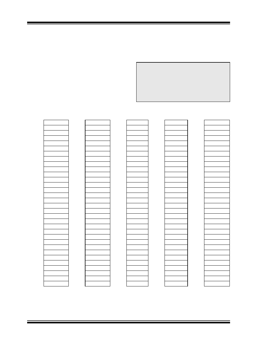
TABLE 6-2:
ACCESS BANK SPECIAL FUNCTION REGISTER MAP
Address
Name
Address
Name
Address
Name
Address
Name
Address
Name
FFFh
TOSU
FDFh
INDF2(1)
FBFh
PSTR1CON
F9Fh
IPR1
F7Fh
SPBRGH1
FFEh
TOSH
FDEh
POSTINC2(1)
FBEh
ECCP1AS
F9Eh
PIR1
F7Eh
BAUDCON1
FFDh
TOSL
FDDh
POSTDEC2(1)
FBDh
ECCP1DEL
F9Dh
PIE1
F7Dh
SPBRGH2
FFCh
STKPTR
FDCh
PREINC2(1)
FBCh
CCPR1H
F9Ch
RCSTA2
F7Ch
BAUDCON2
FFBh
PCLATU
FDBh
PLUSW2(1)
FBBh
CCPR1L
F9Bh
OSCTUNE
F7Bh
TMR3H
FFAh
PCLATH
FDAh
FSR2H
FBAh
CCP1CON
F9Ah
T1GCON
F7Ah
TMR3L
FF9h
PCL
FD9h
FSR2L
FB9h
PSTR2CON
F99h
IPR5
F79h
T3CON
FF8h
TBLPTRU
FD8h
STATUS
FB8h
ECCP2AS
F98h
PIR5
F78h
TMR4
FF7h
TBLPTRH
FD7h
TMR0H
FB7h
ECCP2DEL
F97h
T3GCON
F77h
PR4
FF6h
TBLPTRL
FD6h
TMR0L
FB6h
CCPR2H
F96h
TRISE
F76h
T4CON
FF5h
TABLAT
FD5h
T0CON
FB5h
CCPR2L
F95h
TRISD
F75h
SSP2BUF
FF4h
PRODH
FD4h
—(5)
FB4h
CCP2CON
F94h
TRISC
F74h
SSP2ADD(3)
FF3h
PRODL
FD3h
OSCCON
FB3h CTMUCONH
F93h
TRISB
F73h
SSP2STAT
FF2h
INTCON
FD2h
CM1CON
FB2h CTMUCONL
F92h
TRISA
F72h
SSP2CON1
FF1h
INTCON2
FD1h
CM2CON
FB1h
CTMUICON
F91h
PIE5
F71h
SSP2CON2
FF0h
INTCON3
FD0h
RCON
FB0h
SPBRG1
F90h
IPR4
F70h
CMSTAT
FEFh
INDF0(1)
FCFh
TMR1H
FAFh
RCREG1
F8Fh
PIR4
F6Fh
PMADDRH(2,4)
FEEh
POSTINC0(1)
FCEh
TMR1L
FAEh
TXREG1
F8Eh
PIE4
F6Eh
PMADDRL(2,4)
FEDh
POSTDEC0(1)
FCDh
T1CON
FADh
TXSTA1
F8Dh
LATE(2)
F6Dh
PMDIN1H(2)
FECh
PREINC0(1)
FCCh
TMR2
FACh
RCSTA1
F8Ch
LATD(2)
F6Ch
PMDIN1L(2)
FEBh
PLUSW0(1)
FCBh
PR2
FABh
SPBRG2
F8Bh
LATC
F6Bh
TXADDRL
FEAh
FSR0H
FCAh
T2CON
FAAh
RCREG2
F8Ah
LATB
F6Ah
TXADDRH
FE9h
FSR0L
FC9h
SSP1BUF
FA9h
TXREG2
F89h
LATA
F69h
RXADDRL
FE8h
WREG
FC8h
SSP1ADD(3)
FA8h
TXSTA2
F88h
DMACON1
F68h
RXADDRH
FE7h
INDF1(1)
FC7h
SSP1STAT
FA7h
EECON2
F87h
OSCCON2(5)
F67h
DMABCL
FE6h
POSTINC1(1)
FC6h
SSP1CON1
FA6h
EECON1
F86h
DMACON2
F66h
DMABCH
FE5h
POSTDEC1(1)
FC5h
SSP1CON2
FA5h
IPR3
F85h
HLVDCON
F65h
UCON
FE4h
PREINC1(1)
FC4h
ADRESH
FA4h
PIR3
F84h
PORTE(2)
F64h
USTAT
FE3h
PLUSW1(1)
FC3h
ADRESL
FA3h
PIE3
F83h
PORTD(2)
F63h
UEIR
FE2h
FSR1H
FC2h
ADCON0
FA2h
IPR2
F82h
PORTC
F62h
UIR
FE1h
FSR1L
FC1h
ADCON1
FA1h
PIR2
F81h
PORTB
F61h
UFRMH
FE0h
BSR
FC0h
WDTCON
FA0h
PIE2
F80h
PORTA
F60h
UFRML
Note 1:
This is not a physical register.
2:
This register is not available on 28-pin devices.
3:
SSPxADD and SSPxMSK share the same address.
4:
PMADDRH and PMDOUTH share the same address and PMADDRL and PMDOUTL share the same address.
PMADDRx is used in Master modes and PMDOUTx is used in Slave modes.
5:
Reserved: Do not write to this location.
相关PDF资料 |
PDF描述 |
|---|---|
| PIC18F27J53T-I/SO | IC MCU 8BIT 128KB FLASH 28SOIC |
| VE-J02-IY-B1 | CONVERTER MOD DC/DC 15V 50W |
| VE-J01-IY-B1 | CONVERTER MOD DC/DC 12V 50W |
| PAG.M0.4GL.AC52G | CONN PLUG 4POS STRGHT PIN SOLDER |
| PIC18LF4450T-I/ML | IC PIC MCU FLASH 8KX16 44QFN |
相关代理商/技术参数 |
参数描述 |
|---|---|
| PIC18LF320-I/S0 | 制造商:Microchip Technology Inc 功能描述: |
| PIC18LF4220-I/ML | 功能描述:8位微控制器 -MCU 4KB 512 RAM 36I/O RoHS:否 制造商:Silicon Labs 核心:8051 处理器系列:C8051F39x 数据总线宽度:8 bit 最大时钟频率:50 MHz 程序存储器大小:16 KB 数据 RAM 大小:1 KB 片上 ADC:Yes 工作电源电压:1.8 V to 3.6 V 工作温度范围:- 40 C to + 105 C 封装 / 箱体:QFN-20 安装风格:SMD/SMT |
| PIC18LF4220-I/P | 功能描述:8位微控制器 -MCU 4KB 512 RAM 36I/O RoHS:否 制造商:Silicon Labs 核心:8051 处理器系列:C8051F39x 数据总线宽度:8 bit 最大时钟频率:50 MHz 程序存储器大小:16 KB 数据 RAM 大小:1 KB 片上 ADC:Yes 工作电源电压:1.8 V to 3.6 V 工作温度范围:- 40 C to + 105 C 封装 / 箱体:QFN-20 安装风格:SMD/SMT |
| PIC18LF4220-I/PT | 功能描述:8位微控制器 -MCU 4KB 512 RAM 36I/O RoHS:否 制造商:Silicon Labs 核心:8051 处理器系列:C8051F39x 数据总线宽度:8 bit 最大时钟频率:50 MHz 程序存储器大小:16 KB 数据 RAM 大小:1 KB 片上 ADC:Yes 工作电源电压:1.8 V to 3.6 V 工作温度范围:- 40 C to + 105 C 封装 / 箱体:QFN-20 安装风格:SMD/SMT |
| PIC18LF4220IPT | 制造商:MICROCHIP 功能描述:Pb Free |
发布紧急采购,3分钟左右您将得到回复。