- 您现在的位置:买卖IC网 > PDF目录11450 > PIC18LF27J53T-I/SS (Microchip Technology)IC MCU 8BIT 128KB FLASH 28SSOP PDF资料下载
参数资料
| 型号: | PIC18LF27J53T-I/SS |
| 厂商: | Microchip Technology |
| 文件页数: | 17/389页 |
| 文件大小: | 0K |
| 描述: | IC MCU 8BIT 128KB FLASH 28SSOP |
| 标准包装: | 2,100 |
| 系列: | PIC® XLP™ 18F |
| 核心处理器: | PIC |
| 芯体尺寸: | 8-位 |
| 速度: | 48MHz |
| 连通性: | I²C,LIN,SPI,UART/USART,USB |
| 外围设备: | 欠压检测/复位,POR,PWM,WDT |
| 输入/输出数: | 22 |
| 程序存储器容量: | 128KB(64K x 16) |
| 程序存储器类型: | 闪存 |
| RAM 容量: | 3.8K x 8 |
| 电压 - 电源 (Vcc/Vdd): | 2 V ~ 2.75 V |
| 数据转换器: | A/D 10x10b/12b |
| 振荡器型: | 内部 |
| 工作温度: | -40°C ~ 85°C |
| 封装/外壳: | 28-SSOP(0.209",5.30mm 宽) |
| 包装: | 带卷 (TR) |
第1页第2页第3页第4页第5页第6页第7页第8页第9页第10页第11页第12页第13页第14页第15页第16页当前第17页第18页第19页第20页第21页第22页第23页第24页第25页第26页第27页第28页第29页第30页第31页第32页第33页第34页第35页第36页第37页第38页第39页第40页第41页第42页第43页第44页第45页第46页第47页第48页第49页第50页第51页第52页第53页第54页第55页第56页第57页第58页第59页第60页第61页第62页第63页第64页第65页第66页第67页第68页第69页第70页第71页第72页第73页第74页第75页第76页第77页第78页第79页第80页第81页第82页第83页第84页第85页第86页第87页第88页第89页第90页第91页第92页第93页第94页第95页第96页第97页第98页第99页第100页第101页第102页第103页第104页第105页第106页第107页第108页第109页第110页第111页第112页第113页第114页第115页第116页第117页第118页第119页第120页第121页第122页第123页第124页第125页第126页第127页第128页第129页第130页第131页第132页第133页第134页第135页第136页第137页第138页第139页第140页第141页第142页第143页第144页第145页第146页第147页第148页第149页第150页第151页第152页第153页第154页第155页第156页第157页第158页第159页第160页第161页第162页第163页第164页第165页第166页第167页第168页第169页第170页第171页第172页第173页第174页第175页第176页第177页第178页第179页第180页第181页第182页第183页第184页第185页第186页第187页第188页第189页第190页第191页第192页第193页第194页第195页第196页第197页第198页第199页第200页第201页第202页第203页第204页第205页第206页第207页第208页第209页第210页第211页第212页第213页第214页第215页第216页第217页第218页第219页第220页第221页第222页第223页第224页第225页第226页第227页第228页第229页第230页第231页第232页第233页第234页第235页第236页第237页第238页第239页第240页第241页第242页第243页第244页第245页第246页第247页第248页第249页第250页第251页第252页第253页第254页第255页第256页第257页第258页第259页第260页第261页第262页第263页第264页第265页第266页第267页第268页第269页第270页第271页第272页第273页第274页第275页第276页第277页第278页第279页第280页第281页第282页第283页第284页第285页第286页第287页第288页第289页第290页第291页第292页第293页第294页第295页第296页第297页第298页第299页第300页第301页第302页第303页第304页第305页第306页第307页第308页第309页第310页第311页第312页第313页第314页第315页第316页第317页第318页第319页第320页第321页第322页第323页第324页第325页第326页第327页第328页第329页第330页第331页第332页第333页第334页第335页第336页第337页第338页第339页第340页第341页第342页第343页第344页第345页第346页第347页第348页第349页第350页第351页第352页第353页第354页第355页第356页第357页第358页第359页第360页第361页第362页第363页第364页第365页第366页第367页第368页第369页第370页第371页第372页第373页第374页第375页第376页第377页第378页第379页第380页第381页第382页第383页第384页第385页第386页第387页第388页第389页
2010 Microchip Technology Inc.
DS39774D-page 129
PIC18F85J11 FAMILY
11.0 I/O PORTS
Depending on the device selected and features
enabled, there are up to nine ports available. Some
pins of the I/O ports are multiplexed with an alternate
function from the peripheral features on the device. In
general, when a peripheral is enabled, that pin may not
be used as a general purpose I/O pin.
Each port has three memory mapped registers for its
operation:
TRIS register (Data Direction register)
PORT register (reads the levels on the pins of the
device)
LAT register (Output Latch register)
Reading the PORT register reads the current status of
the pins, whereas writing to the PORT register writes to
the Output Latch (LAT) register.
Setting a TRIS bit (= 1) makes the corresponding
PORT pin an input (i.e., put the corresponding output
driver in a High-Impedance mode). Clearing a TRIS bit
(= 0) makes the corresponding PORT pin an output
(i.e., put the contents of the corresponding LAT bit on
the selected pin).
The Output Latch (LAT register) is useful for
read-modify-write operations on the value that the I/O
pins are driving. Read-modify-write operations on the
LAT register read and write the latched output value for
the PORT register.
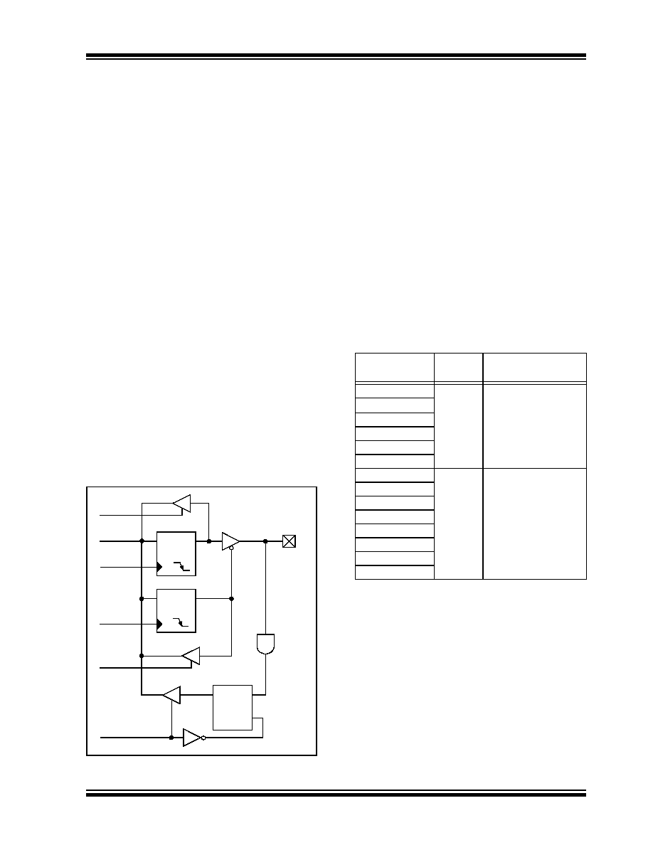
A simplified model of a generic I/O port, without the
interfaces to other peripherals, is shown in Figure 11-1.
FIGURE 11-1:
GENERIC I/O PORT
OPERATION
11.1
I/O Port Pin Capabilities
When developing an application, the capabilities of the
port pins must be considered. Outputs on some pins
have higher output drive strength than others. Similarly,
some pins can tolerate higher than VDD input levels.
11.1.1
INPUT PINS AND VOLTAGE
CONSIDERATIONS
The voltage tolerance of pins used as device inputs is
dependent on the pin’s input function. Most pins that are
used as digital only inputs are able to handle DC
voltages up to 5.5V, a level typical for digital logic
circuits. The digital pins that cannot exceed VDD are
RE0, RE1, RE2, RG0, RG2 and RG3.
In contrast, pins that also have analog input functions of
any kind can only tolerate voltages up to VDD. Voltage
excursions beyond VDD on these pins should be avoided.
Table 11-1 summarizes the input voltage capabilities.
Refer to Section 26.0 “Electrical Characteristics” for
more details.
TABLE 11-1:
INPUT VOLTAGE TOLERANCE
11.1.2
PIN OUTPUT DRIVE
When used as digital I/O, the output pin drive strengths
vary for groups of pins intended to meet the needs for
a variety of applications. In general, there are three
classes of output pins in terms of drive capability.
PORTB and PORTC, as well as PORTA<7:6>, are
designed to drive higher current loads, such as LEDs.
PORTD, PORTE and PORTJ are capable of driving
digital circuits associated with external memory
devices. They can also drive LEDs, but only those with
smaller current requirements. PORTF, PORTG and
PORTH, along with PORTA<5:0>, have the lowest
drive level, but are capable of driving normal digital
circuit loads with a high input impedance.
Data
Bus
WR LAT
WR TRIS
RD PORT
Data Latch
TRIS Latch
RD TRIS
Input
Buffer
I/O pin(1)
Q
D
CK
Q
D
CK
EN
Q
D
EN
RD LAT
or PORT
Port or Pin
Tolerated
Input
Description
PORTA<7:5>
VDD
Only VDD input levels
tolerated.
PORTA<3:0>
PORTC<1:0>
PORTE<2:0>
PORTF<7:1>
PORTG<3:2,0>
PORTA<4>
5.5V
Tolerates input levels
above VDD, useful for
most standard logic.
PORTB<7:0>
PORTC<7:2>
PORTD<7:0>
PORTE<7:3>
PORTG<4,1>
PORTH<7:0>(1)
PORTJ<7:0>(1)
Note 1: Not available on 64-pin devices.
相关PDF资料 |
PDF描述 |
|---|---|
| PIC18F27J53T-I/SS | IC MCU 8BIT 128KB FLASH 28SSOP |
| VE-JNF-IW-S | CONVERTER MOD DC/DC 72V 100W |
| VE-JND-IW-S | CONVERTER MOD DC/DC 85V 100W |
| VE-J6P-IW-S | CONVERTER MOD DC/DC 13.8V 100W |
| PIC18F85K22T-I/PTRSL | MCU 8BIT 32K FLASH 80-TQFP |
相关代理商/技术参数 |
参数描述 |
|---|---|
| PIC18LF320-I/S0 | 制造商:Microchip Technology Inc 功能描述: |
| PIC18LF4220-I/ML | 功能描述:8位微控制器 -MCU 4KB 512 RAM 36I/O RoHS:否 制造商:Silicon Labs 核心:8051 处理器系列:C8051F39x 数据总线宽度:8 bit 最大时钟频率:50 MHz 程序存储器大小:16 KB 数据 RAM 大小:1 KB 片上 ADC:Yes 工作电源电压:1.8 V to 3.6 V 工作温度范围:- 40 C to + 105 C 封装 / 箱体:QFN-20 安装风格:SMD/SMT |
| PIC18LF4220-I/P | 功能描述:8位微控制器 -MCU 4KB 512 RAM 36I/O RoHS:否 制造商:Silicon Labs 核心:8051 处理器系列:C8051F39x 数据总线宽度:8 bit 最大时钟频率:50 MHz 程序存储器大小:16 KB 数据 RAM 大小:1 KB 片上 ADC:Yes 工作电源电压:1.8 V to 3.6 V 工作温度范围:- 40 C to + 105 C 封装 / 箱体:QFN-20 安装风格:SMD/SMT |
| PIC18LF4220-I/PT | 功能描述:8位微控制器 -MCU 4KB 512 RAM 36I/O RoHS:否 制造商:Silicon Labs 核心:8051 处理器系列:C8051F39x 数据总线宽度:8 bit 最大时钟频率:50 MHz 程序存储器大小:16 KB 数据 RAM 大小:1 KB 片上 ADC:Yes 工作电源电压:1.8 V to 3.6 V 工作温度范围:- 40 C to + 105 C 封装 / 箱体:QFN-20 安装风格:SMD/SMT |
| PIC18LF4220IPT | 制造商:MICROCHIP 功能描述:Pb Free |
发布紧急采购,3分钟左右您将得到回复。