- 您现在的位置:买卖IC网 > PDF目录11450 > PIC18LF27J53T-I/SS (Microchip Technology)IC MCU 8BIT 128KB FLASH 28SSOP PDF资料下载
参数资料
| 型号: | PIC18LF27J53T-I/SS |
| 厂商: | Microchip Technology |
| 文件页数: | 170/389页 |
| 文件大小: | 0K |
| 描述: | IC MCU 8BIT 128KB FLASH 28SSOP |
| 标准包装: | 2,100 |
| 系列: | PIC® XLP™ 18F |
| 核心处理器: | PIC |
| 芯体尺寸: | 8-位 |
| 速度: | 48MHz |
| 连通性: | I²C,LIN,SPI,UART/USART,USB |
| 外围设备: | 欠压检测/复位,POR,PWM,WDT |
| 输入/输出数: | 22 |
| 程序存储器容量: | 128KB(64K x 16) |
| 程序存储器类型: | 闪存 |
| RAM 容量: | 3.8K x 8 |
| 电压 - 电源 (Vcc/Vdd): | 2 V ~ 2.75 V |
| 数据转换器: | A/D 10x10b/12b |
| 振荡器型: | 内部 |
| 工作温度: | -40°C ~ 85°C |
| 封装/外壳: | 28-SSOP(0.209",5.30mm 宽) |
| 包装: | 带卷 (TR) |
第1页第2页第3页第4页第5页第6页第7页第8页第9页第10页第11页第12页第13页第14页第15页第16页第17页第18页第19页第20页第21页第22页第23页第24页第25页第26页第27页第28页第29页第30页第31页第32页第33页第34页第35页第36页第37页第38页第39页第40页第41页第42页第43页第44页第45页第46页第47页第48页第49页第50页第51页第52页第53页第54页第55页第56页第57页第58页第59页第60页第61页第62页第63页第64页第65页第66页第67页第68页第69页第70页第71页第72页第73页第74页第75页第76页第77页第78页第79页第80页第81页第82页第83页第84页第85页第86页第87页第88页第89页第90页第91页第92页第93页第94页第95页第96页第97页第98页第99页第100页第101页第102页第103页第104页第105页第106页第107页第108页第109页第110页第111页第112页第113页第114页第115页第116页第117页第118页第119页第120页第121页第122页第123页第124页第125页第126页第127页第128页第129页第130页第131页第132页第133页第134页第135页第136页第137页第138页第139页第140页第141页第142页第143页第144页第145页第146页第147页第148页第149页第150页第151页第152页第153页第154页第155页第156页第157页第158页第159页第160页第161页第162页第163页第164页第165页第166页第167页第168页第169页当前第170页第171页第172页第173页第174页第175页第176页第177页第178页第179页第180页第181页第182页第183页第184页第185页第186页第187页第188页第189页第190页第191页第192页第193页第194页第195页第196页第197页第198页第199页第200页第201页第202页第203页第204页第205页第206页第207页第208页第209页第210页第211页第212页第213页第214页第215页第216页第217页第218页第219页第220页第221页第222页第223页第224页第225页第226页第227页第228页第229页第230页第231页第232页第233页第234页第235页第236页第237页第238页第239页第240页第241页第242页第243页第244页第245页第246页第247页第248页第249页第250页第251页第252页第253页第254页第255页第256页第257页第258页第259页第260页第261页第262页第263页第264页第265页第266页第267页第268页第269页第270页第271页第272页第273页第274页第275页第276页第277页第278页第279页第280页第281页第282页第283页第284页第285页第286页第287页第288页第289页第290页第291页第292页第293页第294页第295页第296页第297页第298页第299页第300页第301页第302页第303页第304页第305页第306页第307页第308页第309页第310页第311页第312页第313页第314页第315页第316页第317页第318页第319页第320页第321页第322页第323页第324页第325页第326页第327页第328页第329页第330页第331页第332页第333页第334页第335页第336页第337页第338页第339页第340页第341页第342页第343页第344页第345页第346页第347页第348页第349页第350页第351页第352页第353页第354页第355页第356页第357页第358页第359页第360页第361页第362页第363页第364页第365页第366页第367页第368页第369页第370页第371页第372页第373页第374页第375页第376页第377页第378页第379页第380页第381页第382页第383页第384页第385页第386页第387页第388页第389页
2010 Microchip Technology Inc.
DS39774D-page 267
PIC18F85J11 FAMILY
20.7
A/D Converter Calibration
The A/D Converter in the PIC18F85J11 family of
devices includes a self-calibration feature which com-
pensates for any offset generated within the module.
The calibration process is automated and is initiated by
setting the ADCAL bit (ADCON0<7>). The next time
the GO/DONE bit is set, the module will perform a
“dummy” conversion (that is, with reading none of the
input channels) and store the resulting value internally
to compensate for offset. Thus, subsequent offsets will
be compensated.
The calibration process assumes that the device is in a
relatively steady-state operating condition. If A/D
calibration is used, it should be performed after each
device Reset or if there are other major changes in
operating conditions.
20.8
Operation in Power-Managed
Modes
The selection of the automatic acquisition time and A/D
conversion clock is determined in part by the clock
source and frequency while in a power-managed
mode.
If the A/D is expected to operate while the device is in
a power-managed mode, the ACQT<2:0> and
ADCS<2:0> bits in ADCON2 should be updated in
accordance with the power-managed mode clock that
will be used. After the power-managed mode is entered
(either of the power-managed Run modes), an A/D
acquisition or conversion may be started. Once an
acquisition or conversion is started, the device should
continue to be clocked by the same power-managed
mode clock source until the conversion has been
completed. If desired, the device may be placed into
the corresponding power-managed Idle mode during
the conversion.
If the power-managed mode clock frequency is less
than 1 MHz, the A/D RC clock source should be
selected.
Operation in the Sleep mode requires the A/D RC clock
to be selected. If bits, ACQT<2:0>, are set to ‘000’ and
a conversion is started, the conversion will be delayed
one instruction cycle to allow execution of the SLEEP
instruction and entry to Sleep mode. The IDLEN and
SCS<1:0> bits in the OSCCON register must have
already been cleared prior to starting the conversion.
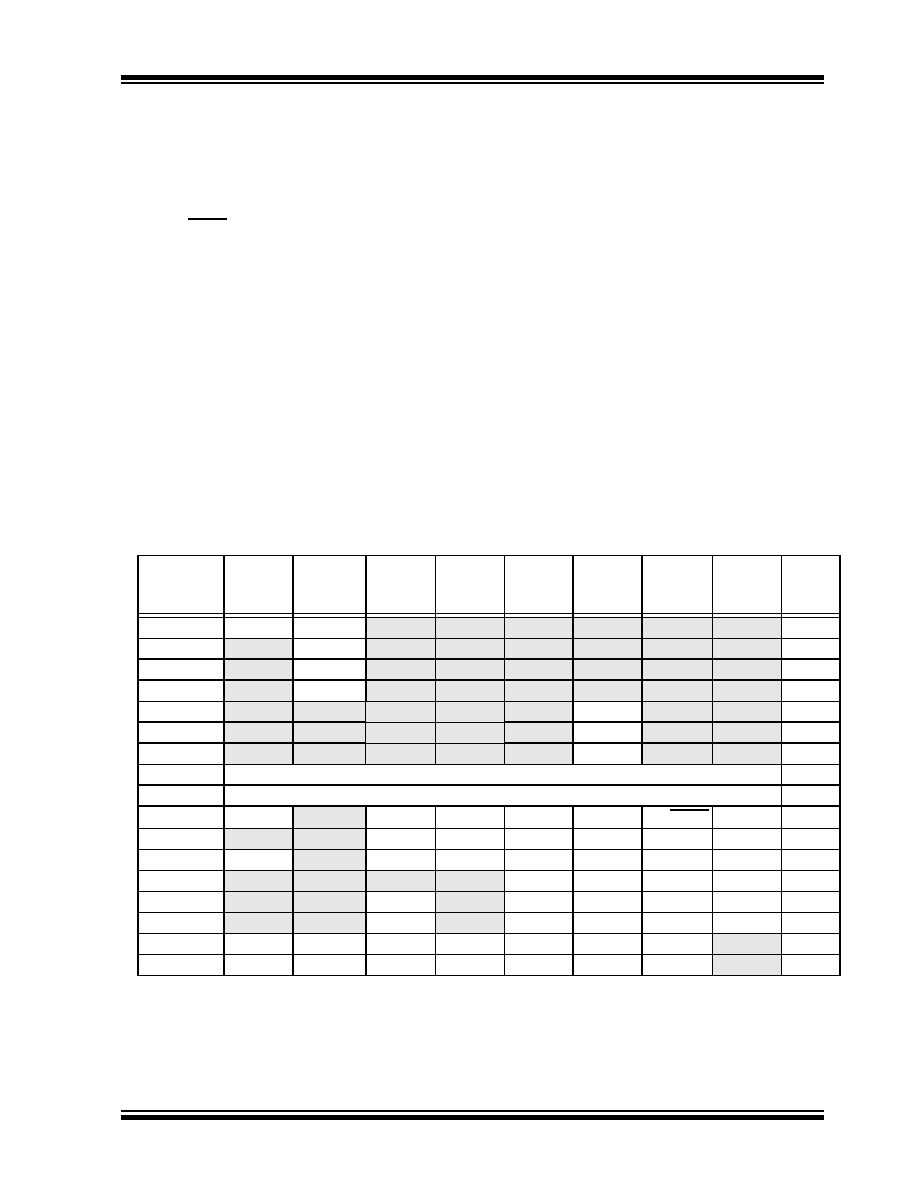
TABLE 20-2:
SUMMARY OF A/D REGISTERS
Name
Bit 7
Bit 6
Bit 5
Bit 4
Bit 3
Bit 2
Bit 1
Bit 0
Reset
Values
on page
INTCON
GIE/GIEH PEIE/GIEL TMR0IE
INT0IE
RBIE
TMR0IF
INT0IF
RBIF
PIR1
PSPIF
ADIF
RC1IF
TX1IF
SSPIF
—
TMR2IF
TMR1IF
PIE1
PSPIE
ADIE
RC1IE
TX1IE
SSPIE
—
TMR2IE
TMR1IE
IPR1
PSPIP
ADIP
RC1IP
TX1IP
SSPIP
—
TMR2IP
TMR1IP
PIR3
—
RC2IF
TX2IF
—
CCP2IF
CCP1IF
PIE3
—
RC2IE
TX2IE
—
CCP2IE
CCP1IE
IPR3
—
RC2IP
TX2IP
—
CCP2IP
CCP1IP
ADRESH
A/D Result Register High Byte
ADRESL
A/D Result Register Low Byte
ADCON0
ADCAL
—
CHS3
CHS2
CHS1
CHS0
GO/DONE
ADON
ADCON1
—
VCFG1
VCFG0
PCFG3
PCFG2
PCFG1
PCFG0
ADCON2
ADFM
—
ACQT2
ACQT1
ACQT0
ADCS2
ADCS1
ADCS0
CCP2CON
—
DC2B1
DC2B0
CCP2M3 CCP2M2 CCP2M1
CCP2M0
PORTA
RA7(1)
RA6(1)
RA5
RA4
RA3
RA2
RA1
RA0
TRISA
TRISA7(1) TRISA6(1)
TRISA5
TRISA4
TRISA3
TRISA2
TRISA1
TRISA0
PORTF
RF7
RF6
RF5
RF4
RF3
RF2
RF1
TRISF
TRISF5
TRISF4
TRISF5
TRISF4
TRISF3
TRISF2
TRISF1
Legend:
— = unimplemented, read as ‘0’. Shaded cells are not used for A/D conversion.
Note 1: RA6/RA7 and their associated latch and direction bits are configured as port pins only when the internal
oscillator is selected as the default clock source (FOSC2 Configuration bit = 0); otherwise, they are
disabled and these bits read as ‘0’.
相关PDF资料 |
PDF描述 |
|---|---|
| PIC18F27J53T-I/SS | IC MCU 8BIT 128KB FLASH 28SSOP |
| VE-JNF-IW-S | CONVERTER MOD DC/DC 72V 100W |
| VE-JND-IW-S | CONVERTER MOD DC/DC 85V 100W |
| VE-J6P-IW-S | CONVERTER MOD DC/DC 13.8V 100W |
| PIC18F85K22T-I/PTRSL | MCU 8BIT 32K FLASH 80-TQFP |
相关代理商/技术参数 |
参数描述 |
|---|---|
| PIC18LF320-I/S0 | 制造商:Microchip Technology Inc 功能描述: |
| PIC18LF4220-I/ML | 功能描述:8位微控制器 -MCU 4KB 512 RAM 36I/O RoHS:否 制造商:Silicon Labs 核心:8051 处理器系列:C8051F39x 数据总线宽度:8 bit 最大时钟频率:50 MHz 程序存储器大小:16 KB 数据 RAM 大小:1 KB 片上 ADC:Yes 工作电源电压:1.8 V to 3.6 V 工作温度范围:- 40 C to + 105 C 封装 / 箱体:QFN-20 安装风格:SMD/SMT |
| PIC18LF4220-I/P | 功能描述:8位微控制器 -MCU 4KB 512 RAM 36I/O RoHS:否 制造商:Silicon Labs 核心:8051 处理器系列:C8051F39x 数据总线宽度:8 bit 最大时钟频率:50 MHz 程序存储器大小:16 KB 数据 RAM 大小:1 KB 片上 ADC:Yes 工作电源电压:1.8 V to 3.6 V 工作温度范围:- 40 C to + 105 C 封装 / 箱体:QFN-20 安装风格:SMD/SMT |
| PIC18LF4220-I/PT | 功能描述:8位微控制器 -MCU 4KB 512 RAM 36I/O RoHS:否 制造商:Silicon Labs 核心:8051 处理器系列:C8051F39x 数据总线宽度:8 bit 最大时钟频率:50 MHz 程序存储器大小:16 KB 数据 RAM 大小:1 KB 片上 ADC:Yes 工作电源电压:1.8 V to 3.6 V 工作温度范围:- 40 C to + 105 C 封装 / 箱体:QFN-20 安装风格:SMD/SMT |
| PIC18LF4220IPT | 制造商:MICROCHIP 功能描述:Pb Free |
发布紧急采购,3分钟左右您将得到回复。