- 您现在的位置:买卖IC网 > PDF目录11299 > PIC18LF4320T-I/ML (Microchip Technology)IC MCU FLASH 4KX16 EEPROM 44QFN PDF资料下载
参数资料
| 型号: | PIC18LF4320T-I/ML |
| 厂商: | Microchip Technology |
| 文件页数: | 239/266页 |
| 文件大小: | 0K |
| 描述: | IC MCU FLASH 4KX16 EEPROM 44QFN |
| 产品培训模块: | Asynchronous Stimulus |
| 标准包装: | 1,600 |
| 系列: | PIC® 18F |
| 核心处理器: | PIC |
| 芯体尺寸: | 8-位 |
| 速度: | 40MHz |
| 连通性: | I²C,SPI,UART/USART |
| 外围设备: | 欠压检测/复位,LVD,POR,PWM,WDT |
| 输入/输出数: | 36 |
| 程序存储器容量: | 8KB(4K x 16) |
| 程序存储器类型: | 闪存 |
| EEPROM 大小: | 256 x 8 |
| RAM 容量: | 512 x 8 |
| 电压 - 电源 (Vcc/Vdd): | 2 V ~ 5.5 V |
| 数据转换器: | A/D 13x10b |
| 振荡器型: | 内部 |
| 工作温度: | -40°C ~ 85°C |
| 封装/外壳: | 44-VQFN 裸露焊盘 |
| 包装: | 带卷 (TR) |
第1页第2页第3页第4页第5页第6页第7页第8页第9页第10页第11页第12页第13页第14页第15页第16页第17页第18页第19页第20页第21页第22页第23页第24页第25页第26页第27页第28页第29页第30页第31页第32页第33页第34页第35页第36页第37页第38页第39页第40页第41页第42页第43页第44页第45页第46页第47页第48页第49页第50页第51页第52页第53页第54页第55页第56页第57页第58页第59页第60页第61页第62页第63页第64页第65页第66页第67页第68页第69页第70页第71页第72页第73页第74页第75页第76页第77页第78页第79页第80页第81页第82页第83页第84页第85页第86页第87页第88页第89页第90页第91页第92页第93页第94页第95页第96页第97页第98页第99页第100页第101页第102页第103页第104页第105页第106页第107页第108页第109页第110页第111页第112页第113页第114页第115页第116页第117页第118页第119页第120页第121页第122页第123页第124页第125页第126页第127页第128页第129页第130页第131页第132页第133页第134页第135页第136页第137页第138页第139页第140页第141页第142页第143页第144页第145页第146页第147页第148页第149页第150页第151页第152页第153页第154页第155页第156页第157页第158页第159页第160页第161页第162页第163页第164页第165页第166页第167页第168页第169页第170页第171页第172页第173页第174页第175页第176页第177页第178页第179页第180页第181页第182页第183页第184页第185页第186页第187页第188页第189页第190页第191页第192页第193页第194页第195页第196页第197页第198页第199页第200页第201页第202页第203页第204页第205页第206页第207页第208页第209页第210页第211页第212页第213页第214页第215页第216页第217页第218页第219页第220页第221页第222页第223页第224页第225页第226页第227页第228页第229页第230页第231页第232页第233页第234页第235页第236页第237页第238页当前第239页第240页第241页第242页第243页第244页第245页第246页第247页第248页第249页第250页第251页第252页第253页第254页第255页第256页第257页第258页第259页第260页第261页第262页第263页第264页第265页第266页
PIC18F2220/2320/4220/4320
DS39599G-page 72
2007 Microchip Technology Inc.
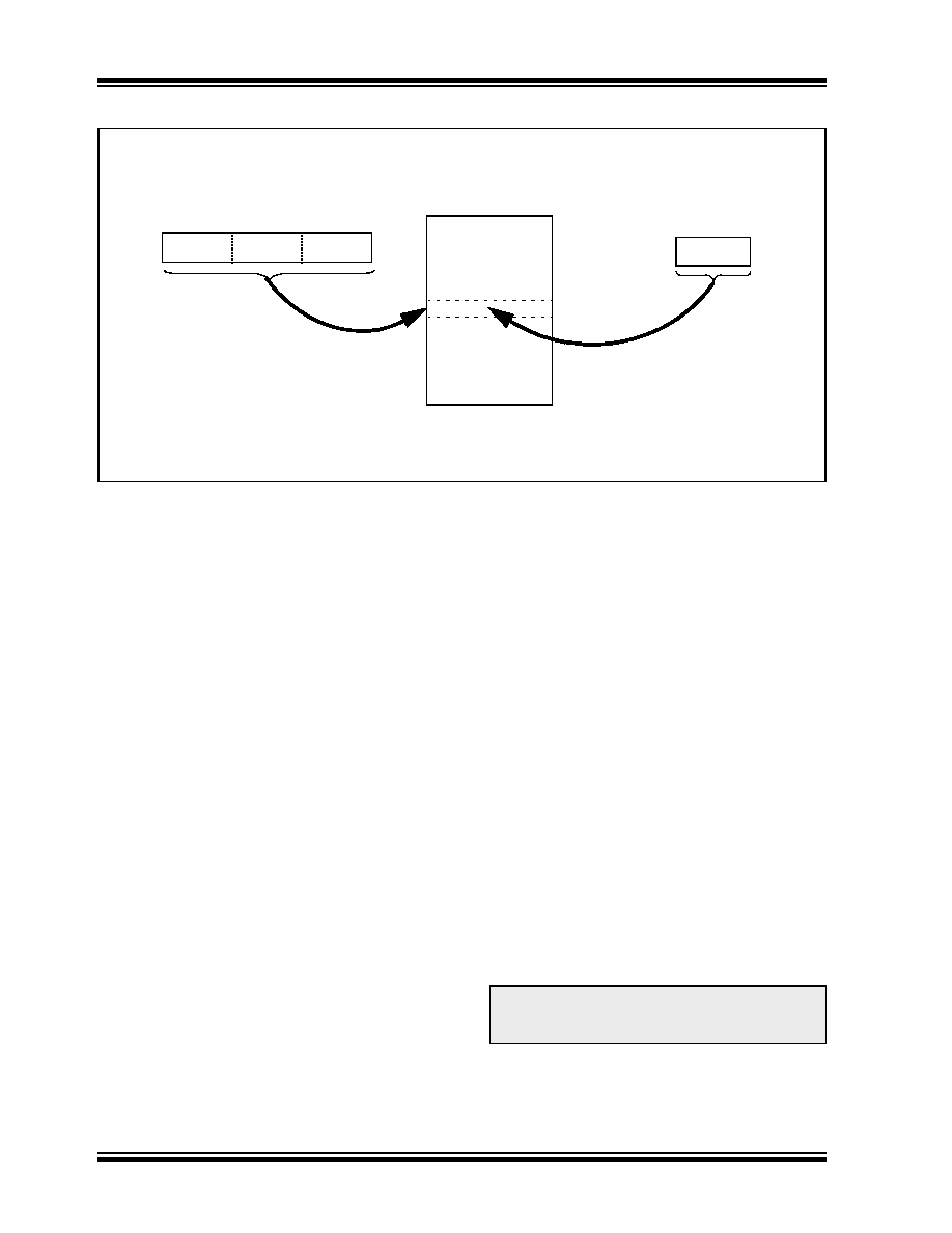
FIGURE 6-2:
TABLE WRITE OPERATION
6.2
Control Registers
Several control registers are used in conjunction with
the TBLRD and TBLWT instructions. These include the:
EECON1 register
EECON2 register
TABLAT register
TBLPTR registers
6.2.1
EECON1 AND EECON2 REGISTERS
EECON1 is the control register for memory accesses.
EECON2 is not a physical register. Reading EECON2
will read all ‘0’s. The EECON2 register is used
exclusively in the memory write and erase sequences.
Control bit, EEPGD, determines if the access will be to
program or data EEPROM memory. When clear,
operations will access the data EEPROM memory.
When set, program memory is accessed.
Control bit, CFGS, determines if the access will be to
the Configuration registers or to program memory/data
EEPROM memory. When set, subsequent operations
access Configuration registers. When CFGS is clear,
the EEPGD bit selects either program Flash or data
EEPROM memory.
The FREE bit controls program memory erase opera-
tions. When the FREE bit is set, the erase operation is
initiated on the next WR command. When FREE is
clear, only writes are enabled.
The WREN bit enables and disables erase and write
operations. When set, erase and write operations are
allowed. When clear, erase and write operations are
disabled – the WR bit cannot be set while the WREN bit
is clear. This process helps to prevent accidental writes
to memory due to errant (unexpected) code execution.
Firmware should keep the WREN bit clear at all times
except when starting erase or write operations. Once
firmware has set the WR bit, the WREN bit may be
cleared. Clearing the WREN bit will not affect the
operation in progress.
The WRERR bit is set when a write operation is inter-
rupted by a Reset. In these situations, the user can
check the WRERR bit and rewrite the location. It will be
necessary to reload the data and address registers
(EEDATA and EEADR) as these registers have cleared
as a result of the Reset.
Control bits, RD and WR, start read and erase/write
operations, respectively. These bits are set by firmware
and cleared by hardware at the completion of the
operation.
The RD bit cannot be set when accessing program
memory (EEPGD = 1). Program memory is read using
table read instructions. See Section 6.3 “Reading the
Flash Program Memory” regarding table reads.
Table Pointer(1)
Table Latch (8-bit)
TBLPTRH
TBLPTRL
TABLAT
Program Memory
(TBLPTR)
TBLPTRU
Instruction: TBLWT*
Note 1: Table Pointer actually points to one of eight holding registers, the address of which is determined by
TBLPTRL<2:0>. The process for physically writing data to the program memory array is discussed in
Holding Registers
Program Memory
Note:
Interrupt flag bit, EEIF in the PIR2 register,
is set when the write is complete. It must
be cleared in software.
相关PDF资料 |
PDF描述 |
|---|---|
| RPE5C2A681J2M1A03A | CAP CER 680PF 100V 5% RADIAL |
| RPE5C2A681J2K1A03B | CAP CER 680PF 100V 5% RADIAL |
| PIC16LC774-I/PQ | IC MCU OTP 4KX14 A/D PWM 44-MQFP |
| GRM31C5C1H104JA01K | CAP CER 0.1UF 50V 5% NP0 1206 |
| PIC16C67-04I/L | IC MCU OTP 8KX14 PWM 44PLCC |
相关代理商/技术参数 |
参数描述 |
|---|---|
| PIC18LF4321-I/ML | 功能描述:8位微控制器 -MCU 44 Pin 4 KB FL 512 RAM RoHS:否 制造商:Silicon Labs 核心:8051 处理器系列:C8051F39x 数据总线宽度:8 bit 最大时钟频率:50 MHz 程序存储器大小:16 KB 数据 RAM 大小:1 KB 片上 ADC:Yes 工作电源电压:1.8 V to 3.6 V 工作温度范围:- 40 C to + 105 C 封装 / 箱体:QFN-20 安装风格:SMD/SMT |
| PIC18LF4321-I/P | 功能描述:8位微控制器 -MCU 40 Pin 4 KB FL 512 RAM RoHS:否 制造商:Silicon Labs 核心:8051 处理器系列:C8051F39x 数据总线宽度:8 bit 最大时钟频率:50 MHz 程序存储器大小:16 KB 数据 RAM 大小:1 KB 片上 ADC:Yes 工作电源电压:1.8 V to 3.6 V 工作温度范围:- 40 C to + 105 C 封装 / 箱体:QFN-20 安装风格:SMD/SMT |
| PIC18LF4321-I/PT | 功能描述:8位微控制器 -MCU 4KB FL 512 RAM RoHS:否 制造商:Silicon Labs 核心:8051 处理器系列:C8051F39x 数据总线宽度:8 bit 最大时钟频率:50 MHz 程序存储器大小:16 KB 数据 RAM 大小:1 KB 片上 ADC:Yes 工作电源电压:1.8 V to 3.6 V 工作温度范围:- 40 C to + 105 C 封装 / 箱体:QFN-20 安装风格:SMD/SMT |
| PIC18LF4321T-I/ML | 功能描述:8位微控制器 -MCU 44 Pin 4 KB FL 512 RAM RoHS:否 制造商:Silicon Labs 核心:8051 处理器系列:C8051F39x 数据总线宽度:8 bit 最大时钟频率:50 MHz 程序存储器大小:16 KB 数据 RAM 大小:1 KB 片上 ADC:Yes 工作电源电压:1.8 V to 3.6 V 工作温度范围:- 40 C to + 105 C 封装 / 箱体:QFN-20 安装风格:SMD/SMT |
| PIC18LF4321T-I/PT | 功能描述:8位微控制器 -MCU 4KB FL 512 RAM RoHS:否 制造商:Silicon Labs 核心:8051 处理器系列:C8051F39x 数据总线宽度:8 bit 最大时钟频率:50 MHz 程序存储器大小:16 KB 数据 RAM 大小:1 KB 片上 ADC:Yes 工作电源电压:1.8 V to 3.6 V 工作温度范围:- 40 C to + 105 C 封装 / 箱体:QFN-20 安装风格:SMD/SMT |
发布紧急采购,3分钟左右您将得到回复。