- 您现在的位置:买卖IC网 > PDF目录11299 > PIC18LF4320T-I/ML (Microchip Technology)IC MCU FLASH 4KX16 EEPROM 44QFN PDF资料下载
参数资料
| 型号: | PIC18LF4320T-I/ML |
| 厂商: | Microchip Technology |
| 文件页数: | 9/266页 |
| 文件大小: | 0K |
| 描述: | IC MCU FLASH 4KX16 EEPROM 44QFN |
| 产品培训模块: | Asynchronous Stimulus |
| 标准包装: | 1,600 |
| 系列: | PIC® 18F |
| 核心处理器: | PIC |
| 芯体尺寸: | 8-位 |
| 速度: | 40MHz |
| 连通性: | I²C,SPI,UART/USART |
| 外围设备: | 欠压检测/复位,LVD,POR,PWM,WDT |
| 输入/输出数: | 36 |
| 程序存储器容量: | 8KB(4K x 16) |
| 程序存储器类型: | 闪存 |
| EEPROM 大小: | 256 x 8 |
| RAM 容量: | 512 x 8 |
| 电压 - 电源 (Vcc/Vdd): | 2 V ~ 5.5 V |
| 数据转换器: | A/D 13x10b |
| 振荡器型: | 内部 |
| 工作温度: | -40°C ~ 85°C |
| 封装/外壳: | 44-VQFN 裸露焊盘 |
| 包装: | 带卷 (TR) |
第1页第2页第3页第4页第5页第6页第7页第8页当前第9页第10页第11页第12页第13页第14页第15页第16页第17页第18页第19页第20页第21页第22页第23页第24页第25页第26页第27页第28页第29页第30页第31页第32页第33页第34页第35页第36页第37页第38页第39页第40页第41页第42页第43页第44页第45页第46页第47页第48页第49页第50页第51页第52页第53页第54页第55页第56页第57页第58页第59页第60页第61页第62页第63页第64页第65页第66页第67页第68页第69页第70页第71页第72页第73页第74页第75页第76页第77页第78页第79页第80页第81页第82页第83页第84页第85页第86页第87页第88页第89页第90页第91页第92页第93页第94页第95页第96页第97页第98页第99页第100页第101页第102页第103页第104页第105页第106页第107页第108页第109页第110页第111页第112页第113页第114页第115页第116页第117页第118页第119页第120页第121页第122页第123页第124页第125页第126页第127页第128页第129页第130页第131页第132页第133页第134页第135页第136页第137页第138页第139页第140页第141页第142页第143页第144页第145页第146页第147页第148页第149页第150页第151页第152页第153页第154页第155页第156页第157页第158页第159页第160页第161页第162页第163页第164页第165页第166页第167页第168页第169页第170页第171页第172页第173页第174页第175页第176页第177页第178页第179页第180页第181页第182页第183页第184页第185页第186页第187页第188页第189页第190页第191页第192页第193页第194页第195页第196页第197页第198页第199页第200页第201页第202页第203页第204页第205页第206页第207页第208页第209页第210页第211页第212页第213页第214页第215页第216页第217页第218页第219页第220页第221页第222页第223页第224页第225页第226页第227页第228页第229页第230页第231页第232页第233页第234页第235页第236页第237页第238页第239页第240页第241页第242页第243页第244页第245页第246页第247页第248页第249页第250页第251页第252页第253页第254页第255页第256页第257页第258页第259页第260页第261页第262页第263页第264页第265页第266页
PIC18F2220/2320/4220/4320
DS39599G-page 104
2007 Microchip Technology Inc.
10.2
PORTB, TRISB and LATB
Registers
PORTB is an 8-bit wide, bidirectional port. The corre-
sponding Data Direction register is TRISB. Setting a
TRISB bit (= 1) will make the corresponding PORTB
pin an input (i.e., put the corresponding output driver in
a high-impedance mode). Clearing a TRISB bit (= 0)
will make the corresponding PORTB pin an output (i.e.,
put the contents of the output latch on the selected pin).
The Data Latch register (LATB) is also memory
mapped. Read-modify-write operations on the LATB
register read and write the latched output value for
PORTB.
EXAMPLE 10-2:
INITIALIZING PORTB
Each of the PORTB pins has a weak internal pull-up. A
single control bit can turn on all the pull-ups. This is per-
formed by clearing bit RBPU (INTCON2<7>). The
weak pull-up is automatically turned off when the port
pin is configured as an output. The pull-ups are
disabled on a Power-on Reset.
Four of the PORTB pins (RB7:RB4) have an interrupt-
on-change feature. Only pins configured as inputs can
cause this interrupt to occur (i.e., any RB7:RB4 pin
configured as an output is excluded from the interrupt-
on-change comparison). The input pins (of RB7:RB4)
are compared with the old value latched on the last
read of PORTB. The “mismatch” outputs of RB7:RB4
are OR’ed together to generate the RB Port Change
Interrupt with Flag bit, RBIF (INTCON<0>).
This interrupt can wake the device from Sleep. The
user, in the Interrupt Service Routine, can clear the
interrupt in the following manner:
a) Any read or write of PORTB (except with the
MOVFF (ANY), PORTB instruction). This will
end the mismatch condition.
b) Clear flag bit RBIF.
A mismatch condition will continue to set flag bit RBIF.
Reading PORTB will end the mismatch condition and
allow flag bit RBIF to be cleared.
The interrupt-on-change feature is recommended for
wake-up on key depression operation and operations
where PORTB is only used for the interrupt-on-change
feature. Polling of PORTB is not recommended while
using the interrupt-on-change feature.
RB3 can be configured by the Configuration bit,
CCP2MX, as the alternate peripheral pin for the CCP2
module (CCP2MX = 0).
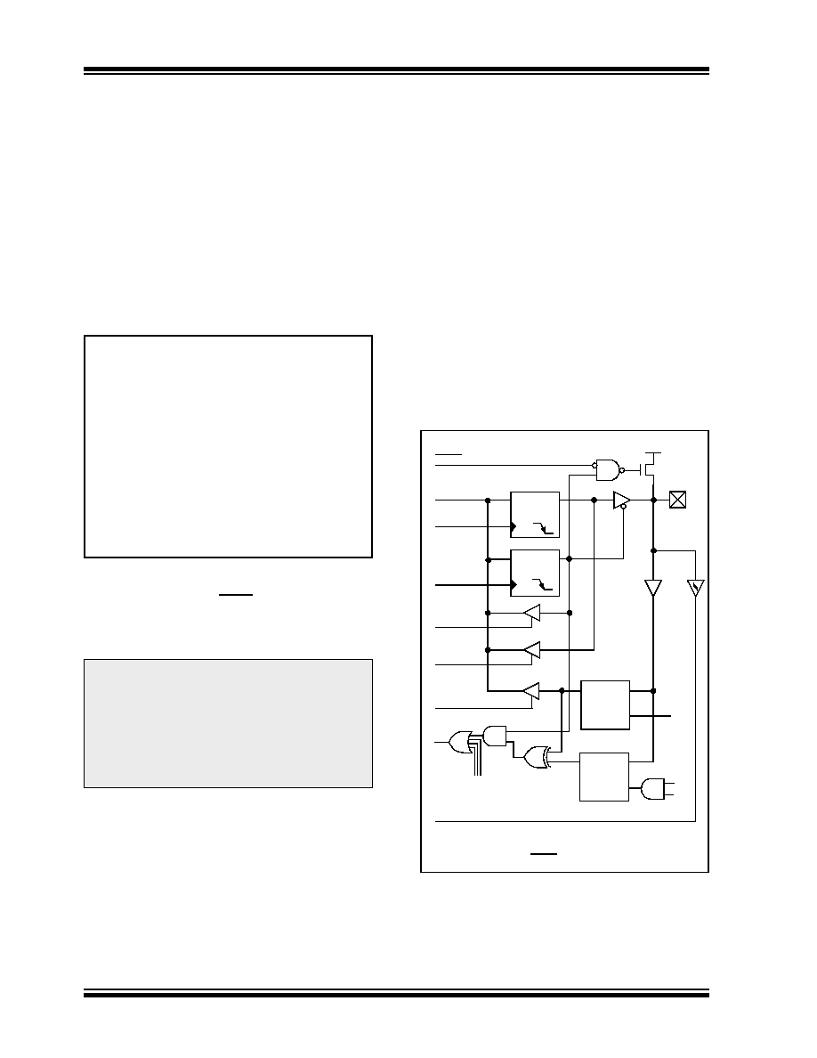
FIGURE 10-6:
BLOCK DIAGRAM OF
RB7:RB5 PINS
Note:
On a Power-on Reset, RB4:RB0 are con-
figured as analog inputs by default and
read as ‘0’; RB7:RB5 are configured as
digital inputs.
By programming the Configuration bit,
PBADEN (CONFIG3H<1>), RB4:RB0 will
alternatively be configured as digital inputs
on POR.
CLRF
PORTB
;
Initialize PORTB by
;
clearing output
;
data latches
CLRF
LATB
;
Alternate method
;
to clear output
;
data latches
MOVLW
0x07
;
Set RB<4:0> as
MOVWF
ADCON1 ;
digital I/O pins
MOVLW
0xCF
;
Value used to
;
initialize data
;
direction
MOVWF
TRISB
;
Set RB<3:0> as inputs
;
RB<5:4> as outputs
;
RB<7:6> as inputs
Data Latch
From other
RBPU(2)
P
VDD
I/O pin(1)
Q
D
CK
Q
D
CK
QD
EN
QD
EN
Data Bus
WR LATB
WR TRISB
Set RBIF
TRIS Latch
RD TRISB
RD PORTB
RB7:RB5 and
Weak
Pull-up
RD PORTB
Latch
TTL
Input
Buffer
ST
Buffer
RB7:RB5 in Serial Programming Mode
Q3
Q1
RD LATB
or PORTB
Note 1:
I/O pins have diode protection to VDD and VSS.
2:
To enable weak pull-ups, set the appropriate TRIS bit(s)
and clear the RBPU bit (INTCON2<7>).
RB4 pins
相关PDF资料 |
PDF描述 |
|---|---|
| RPE5C2A681J2M1A03A | CAP CER 680PF 100V 5% RADIAL |
| RPE5C2A681J2K1A03B | CAP CER 680PF 100V 5% RADIAL |
| PIC16LC774-I/PQ | IC MCU OTP 4KX14 A/D PWM 44-MQFP |
| GRM31C5C1H104JA01K | CAP CER 0.1UF 50V 5% NP0 1206 |
| PIC16C67-04I/L | IC MCU OTP 8KX14 PWM 44PLCC |
相关代理商/技术参数 |
参数描述 |
|---|---|
| PIC18LF4321-I/ML | 功能描述:8位微控制器 -MCU 44 Pin 4 KB FL 512 RAM RoHS:否 制造商:Silicon Labs 核心:8051 处理器系列:C8051F39x 数据总线宽度:8 bit 最大时钟频率:50 MHz 程序存储器大小:16 KB 数据 RAM 大小:1 KB 片上 ADC:Yes 工作电源电压:1.8 V to 3.6 V 工作温度范围:- 40 C to + 105 C 封装 / 箱体:QFN-20 安装风格:SMD/SMT |
| PIC18LF4321-I/P | 功能描述:8位微控制器 -MCU 40 Pin 4 KB FL 512 RAM RoHS:否 制造商:Silicon Labs 核心:8051 处理器系列:C8051F39x 数据总线宽度:8 bit 最大时钟频率:50 MHz 程序存储器大小:16 KB 数据 RAM 大小:1 KB 片上 ADC:Yes 工作电源电压:1.8 V to 3.6 V 工作温度范围:- 40 C to + 105 C 封装 / 箱体:QFN-20 安装风格:SMD/SMT |
| PIC18LF4321-I/PT | 功能描述:8位微控制器 -MCU 4KB FL 512 RAM RoHS:否 制造商:Silicon Labs 核心:8051 处理器系列:C8051F39x 数据总线宽度:8 bit 最大时钟频率:50 MHz 程序存储器大小:16 KB 数据 RAM 大小:1 KB 片上 ADC:Yes 工作电源电压:1.8 V to 3.6 V 工作温度范围:- 40 C to + 105 C 封装 / 箱体:QFN-20 安装风格:SMD/SMT |
| PIC18LF4321T-I/ML | 功能描述:8位微控制器 -MCU 44 Pin 4 KB FL 512 RAM RoHS:否 制造商:Silicon Labs 核心:8051 处理器系列:C8051F39x 数据总线宽度:8 bit 最大时钟频率:50 MHz 程序存储器大小:16 KB 数据 RAM 大小:1 KB 片上 ADC:Yes 工作电源电压:1.8 V to 3.6 V 工作温度范围:- 40 C to + 105 C 封装 / 箱体:QFN-20 安装风格:SMD/SMT |
| PIC18LF4321T-I/PT | 功能描述:8位微控制器 -MCU 4KB FL 512 RAM RoHS:否 制造商:Silicon Labs 核心:8051 处理器系列:C8051F39x 数据总线宽度:8 bit 最大时钟频率:50 MHz 程序存储器大小:16 KB 数据 RAM 大小:1 KB 片上 ADC:Yes 工作电源电压:1.8 V to 3.6 V 工作温度范围:- 40 C to + 105 C 封装 / 箱体:QFN-20 安装风格:SMD/SMT |
发布紧急采购,3分钟左右您将得到回复。