- 您现在的位置:买卖IC网 > PDF目录11313 > PIC18LF4585T-I/PT (Microchip Technology)IC MCU FLASH 24KX16 44TQFP PDF资料下载
参数资料
| 型号: | PIC18LF4585T-I/PT |
| 厂商: | Microchip Technology |
| 文件页数: | 308/322页 |
| 文件大小: | 0K |
| 描述: | IC MCU FLASH 24KX16 44TQFP |
| 产品培训模块: | Asynchronous Stimulus |
| 标准包装: | 1,200 |
| 系列: | PIC® 18F |
| 核心处理器: | PIC |
| 芯体尺寸: | 8-位 |
| 速度: | 40MHz |
| 连通性: | CAN,I²C,SPI,UART/USART |
| 外围设备: | 欠压检测/复位,HLVD,POR,PWM,WDT |
| 输入/输出数: | 36 |
| 程序存储器容量: | 48KB(24K x 16) |
| 程序存储器类型: | 闪存 |
| EEPROM 大小: | 1K x 8 |
| RAM 容量: | 3.25K x 8 |
| 电压 - 电源 (Vcc/Vdd): | 2 V ~ 5.5 V |
| 数据转换器: | A/D 11x10b |
| 振荡器型: | 内部 |
| 工作温度: | -40°C ~ 85°C |
| 封装/外壳: | 44-TQFP |
| 包装: | 带卷 (TR) |
第1页第2页第3页第4页第5页第6页第7页第8页第9页第10页第11页第12页第13页第14页第15页第16页第17页第18页第19页第20页第21页第22页第23页第24页第25页第26页第27页第28页第29页第30页第31页第32页第33页第34页第35页第36页第37页第38页第39页第40页第41页第42页第43页第44页第45页第46页第47页第48页第49页第50页第51页第52页第53页第54页第55页第56页第57页第58页第59页第60页第61页第62页第63页第64页第65页第66页第67页第68页第69页第70页第71页第72页第73页第74页第75页第76页第77页第78页第79页第80页第81页第82页第83页第84页第85页第86页第87页第88页第89页第90页第91页第92页第93页第94页第95页第96页第97页第98页第99页第100页第101页第102页第103页第104页第105页第106页第107页第108页第109页第110页第111页第112页第113页第114页第115页第116页第117页第118页第119页第120页第121页第122页第123页第124页第125页第126页第127页第128页第129页第130页第131页第132页第133页第134页第135页第136页第137页第138页第139页第140页第141页第142页第143页第144页第145页第146页第147页第148页第149页第150页第151页第152页第153页第154页第155页第156页第157页第158页第159页第160页第161页第162页第163页第164页第165页第166页第167页第168页第169页第170页第171页第172页第173页第174页第175页第176页第177页第178页第179页第180页第181页第182页第183页第184页第185页第186页第187页第188页第189页第190页第191页第192页第193页第194页第195页第196页第197页第198页第199页第200页第201页第202页第203页第204页第205页第206页第207页第208页第209页第210页第211页第212页第213页第214页第215页第216页第217页第218页第219页第220页第221页第222页第223页第224页第225页第226页第227页第228页第229页第230页第231页第232页第233页第234页第235页第236页第237页第238页第239页第240页第241页第242页第243页第244页第245页第246页第247页第248页第249页第250页第251页第252页第253页第254页第255页第256页第257页第258页第259页第260页第261页第262页第263页第264页第265页第266页第267页第268页第269页第270页第271页第272页第273页第274页第275页第276页第277页第278页第279页第280页第281页第282页第283页第284页第285页第286页第287页第288页第289页第290页第291页第292页第293页第294页第295页第296页第297页第298页第299页第300页第301页第302页第303页第304页第305页第306页第307页当前第308页第309页第310页第311页第312页第313页第314页第315页第316页第317页第318页第319页第320页第321页第322页
PIC18F2585/2680/4585/4680
DS39625C-page 84
Preliminary
2007 Microchip Technology Inc.
B2DLC(8)
Receive mode
—
RXRTR
RB1
RB0
DLC3
DLC2
DLC1
DLC0
-xxx xxxx
B2DLC(8)
Transmit mode
—TXRTR
—
DLC3
DLC2
DLC1
DLC0
-x-- xxxx
B2EIDL(8)
EID7
EID6
EID5
EID4
EID3
EID2
EID1
EID0
xxxx xxxx
B2EIDH(8)
EID15
EID14
EID13
EID12
EID11
EID10
EID9
EID8
xxxx xxxx
B2SIDL(8)
Receive mode
SID2
SID1
SID0
SRR
EXID
—EID17
EID16
xxxx x-xx
B2SIDL(8)
Transmit mode
SID2
SID1
SID0
—
EXIDE
—EID17
EID16
xxx- x-xx
B2SIDH(8)
SID10
SID9
SID8
SID7
SID6
SID5
SID4
SID3
xxxx xxxx
B2CON(8)
Receive mode
RXFUL
RXM1
RXRTRRO
FILHIT4
FILHIT3
FILHIT2
FILHIT1
FILHIT0
0000 0000
B2CON(8)
Transmit mode
TXBIF
RXM1
TXLARB
TXERR
TXREQ
RTREN
TXPRI1
TXPRI0
0000 0000
B1D7(8)
B1D77
B1D76
B1D75
B1D74
B1D73
B1D72
B1D71
B1D70
xxxx xxxx
B1D6(8)
B1D67
B1D66
B1D65
B1D64
B1D63
B1D62
B1D61
B1D60
xxxx xxxx
B1D5(8)
B1D57
B1D56
B1D55
B1D54
B1D53
B1D52
B1D51
B1D50
xxxx xxxx
B1D4(8)
B1D47
B1D46
B1D45
B1D44
B1D43
B1D42
B1D41
B1D40
xxxx xxxx
B1D3(8)
B1D37
B1D36
B1D35
B1D34
B1D33
B1D32
B1D31
B1D30
xxxx xxxx
B1D2(8)
B1D27
B1D26
B1D25
B1D24
B1D23
B1D22
B1D21
B1D20
xxxx xxxx
B1D1(8)
B1D17
B1D16
B1D15
B1D14
B1D13
B1D12
B1D11
B1D10
xxxx xxxx
B1D0(8)
B1D07
B1D06
B1D05
B1D04
B1D03
B1D02
B1D01
B1D00
xxxx xxxx
B1DLC(8)
Receive mode
—
RXRTR
RB1
RB0
DLC3
DLC2
DLC1
DLC0
-xxx xxxx
B1DLC(8)
Transmit mode
—TXRTR
—
DLC3
DLC2
DLC1
DLC0
-x-- xxxx
B1EIDL(8)
EID7
EID6
EID5
EID4
EID3
EID2
EID1
EID0
xxxx xxxx
B1EIDH(8)
EID15
EID14
EID13
EID12
EID11
EID10
EID9
EID8
xxxx xxxx
B1SIDL(8)
Receive mode
SID2
SID1
SID0
SRR
EXID
—EID17
EID16
xxxx x-xx
B1SIDL(8)
Transmit mode
SID2
SID1
SID0
—
EXIDE
—EID17
EID16
xxx- x-xx
B1SIDH(8)
SID10
SID9
SID8
SID7
SID6
SID5
SID4
SID3
xxxx xxxx
B1CON(8)
Receive mode
RXFUL
RXM1
RXRTRRO
FILHIT4
FILHIT3
FILHIT2
FILHIT1
FILHIT0
0000 0000
B1CON(8)
Transmit mode
TXBIF
TXABT
TXLARB
TXERR
TXREQ
RTREN
TXPRI1
TXPRI0
0000 0000
B0D7(8)
B0D77
B0D76
B0D75
B0D74
B0D73
B0D72
B0D71
B0D70
xxxx xxxx
B0D6(8)
B0D67
B0D66
B0D65
B0D64
B0D63
B0D62
B0D61
B0D60
xxxx xxxx
B0D5(8)
B0D57
B0D56
B0D55
B0D54
B0D53
B0D52
B0D51
B0D50
xxxx xxxx
B0D4(8)
B0D47
B0D46
B0D45
B0D44
B0D43
B0D42
B0D41
B0D40
xxxx xxxx
B0D3(8)
B0D37
B0D36
B0D35
B0D34
B0D33
B0D32
B0D31
B0D30
xxxx xxxx
B0D2(8)
B0D27
B0D26
B0D25
B0D24
B0D23
B0D22
B0D21
B0D20
xxxx xxxx
B0D1(8)
B0D17
B0D16
B0D15
B0D14
B0D13
B0D12
B0D11
B0D10
xxxx xxxx
B0D0(8)
B0D07
B0D06
B0D05
B0D04
B0D03
B0D02
B0D01
B0D00
xxxx xxxx
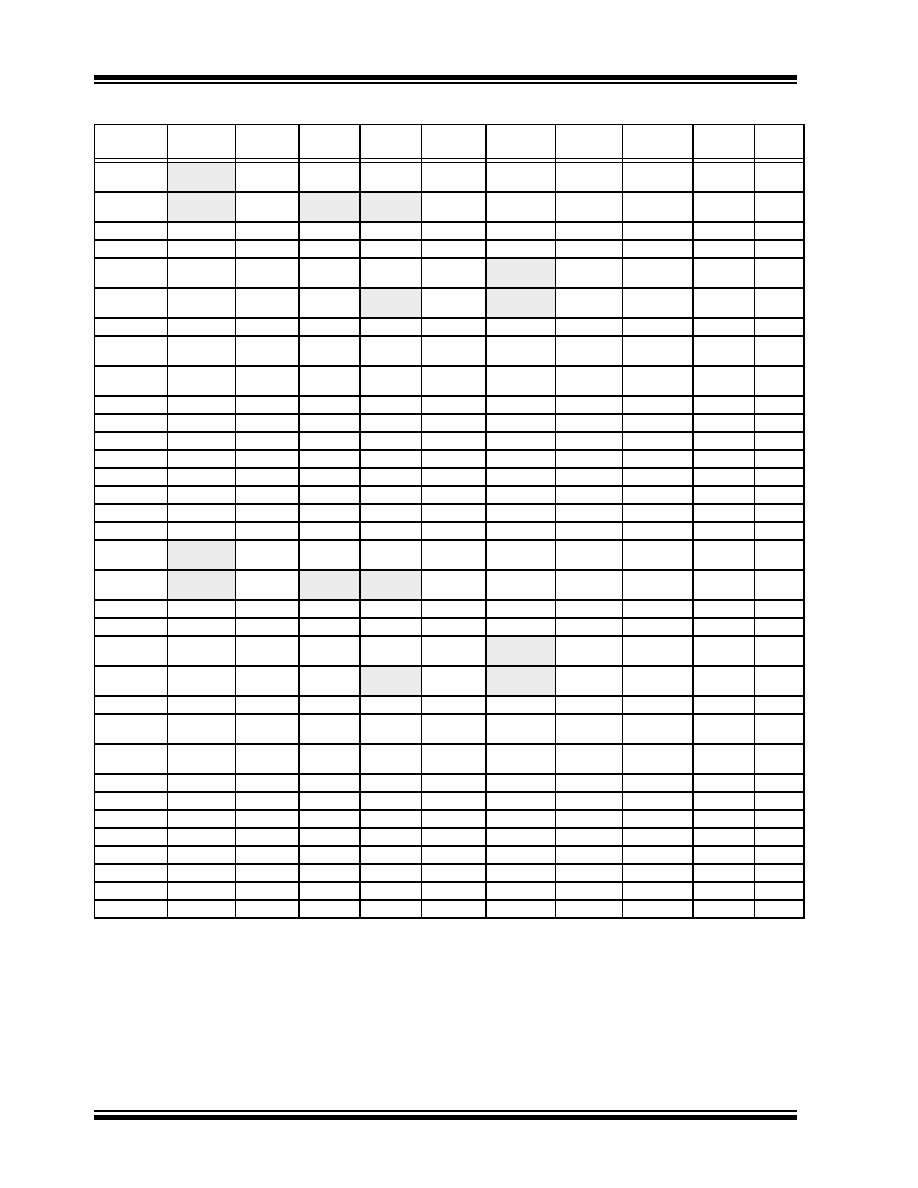
TABLE 5-2:
REGISTER FILE SUMMARY (PIC18F2585/2680/4585/4680) (CONTINUED)
File Name
Bit 7
Bit 6
Bit 5
Bit 4
Bit 3
Bit 2
Bit 1
Bit 0
Value on
POR, BOR
Details
on page:
Legend: x = unknown, u = unchanged, - = unimplemented, q = value depends on condition
Note 1:
Bit 21 of the PC is only available in Test mode and Serial Programming modes.
2:
The SBOREN bit is only available when CONFIG2L<1:0> = 01; otherwise, it is disabled and reads as ‘0’. See Section 4.4 “Brown-out Reset
(BOR)”.
3:
These registers and/or bits are not implemented on PIC18F2X8X devices and are read as ‘0’. Reset values are shown for PIC18F4X8X
devices; individual unimplemented bits should be interpreted as ‘—’.
4:
The PLLEN bit is only available in specific oscillator configuration; otherwise, it is disabled and reads as ‘0’. See Section 2.6.4 “PLL in
INTOSC Modes”.
5:
The RE3 bit is only available when Master Clear Reset is disabled (CONFIG3H<7> = 0); otherwise, RE3 reads as ‘0’. This bit is read-only.
6:
RA6/RA7 and their associated latch and direction bits are individually configured as port pins based on various primary oscillator modes.
When disabled, these bits read as ‘0’.
7:
CAN bits have multiple functions depending on the selected mode of the CAN module.
8:
This register reads all ‘0’s until the ECAN technology is set up in Mode 1 or Mode 2.
9:
These registers are available on PIC18F4X8X devices only.
相关PDF资料 |
PDF描述 |
|---|---|
| RPE5C1H5R0C2P1B03B | CAP CER 5PF 50V RADIAL |
| VE-25V-IX-F1 | CONVERTER MOD DC/DC 5.8V 75W |
| VE-25T-IX-F4 | CONVERTER MOD DC/DC 6.5V 75W |
| RPE5C1H391J2M1A03A | CAP CER 390PF 50V 5% RADIAL |
| RPE5C1H331J2S1A03A | CAP CER 330PF 50V 5% RADIAL |
相关代理商/技术参数 |
参数描述 |
|---|---|
| PIC18LF458-I/L | 功能描述:8位微控制器 -MCU 32KB 1536 RAM 34I/O RoHS:否 制造商:Silicon Labs 核心:8051 处理器系列:C8051F39x 数据总线宽度:8 bit 最大时钟频率:50 MHz 程序存储器大小:16 KB 数据 RAM 大小:1 KB 片上 ADC:Yes 工作电源电压:1.8 V to 3.6 V 工作温度范围:- 40 C to + 105 C 封装 / 箱体:QFN-20 安装风格:SMD/SMT |
| PIC18LF458-I/L | 制造商:Microchip Technology Inc 功能描述:IC 8BIT FLASH MCU 18LF458 PLCC44 |
| PIC18LF458-I/P | 功能描述:8位微控制器 -MCU 32KB 1536 RAM 34I/O RoHS:否 制造商:Silicon Labs 核心:8051 处理器系列:C8051F39x 数据总线宽度:8 bit 最大时钟频率:50 MHz 程序存储器大小:16 KB 数据 RAM 大小:1 KB 片上 ADC:Yes 工作电源电压:1.8 V to 3.6 V 工作温度范围:- 40 C to + 105 C 封装 / 箱体:QFN-20 安装风格:SMD/SMT |
| PIC18LF458-I/P | 制造商:Microchip Technology Inc 功能描述:IC 8BIT FLASH MCU 18LF458 DIP40 |
| PIC18LF458-I/PT | 功能描述:8位微控制器 -MCU 32KB 1536 RAM 34I/O RoHS:否 制造商:Silicon Labs 核心:8051 处理器系列:C8051F39x 数据总线宽度:8 bit 最大时钟频率:50 MHz 程序存储器大小:16 KB 数据 RAM 大小:1 KB 片上 ADC:Yes 工作电源电压:1.8 V to 3.6 V 工作温度范围:- 40 C to + 105 C 封装 / 箱体:QFN-20 安装风格:SMD/SMT |
发布紧急采购,3分钟左右您将得到回复。