- 您现在的位置:买卖IC网 > PDF目录3808 > PIC18LF4685-I/PT (Microchip Technology)IC PIC MCU FLASH 48KX16 44TQFP PDF资料下载
参数资料
| 型号: | PIC18LF4685-I/PT |
| 厂商: | Microchip Technology |
| 文件页数: | 116/183页 |
| 文件大小: | 0K |
| 描述: | IC PIC MCU FLASH 48KX16 44TQFP |
| 产品培训模块: | Asynchronous Stimulus 8-bit PIC® Microcontroller Portfolio |
| 标准包装: | 160 |
| 系列: | PIC® 18F |
| 核心处理器: | PIC |
| 芯体尺寸: | 8-位 |
| 速度: | 40MHz |
| 连通性: | CAN,I²C,SPI,UART/USART |
| 外围设备: | 欠压检测/复位,HLVD,POR,PWM,WDT |
| 输入/输出数: | 36 |
| 程序存储器容量: | 96KB(48K x 16) |
| 程序存储器类型: | 闪存 |
| EEPROM 大小: | 1K x 8 |
| RAM 容量: | 3.25K x 8 |
| 电压 - 电源 (Vcc/Vdd): | 2 V ~ 5.5 V |
| 数据转换器: | A/D 11x10b |
| 振荡器型: | 内部 |
| 工作温度: | -40°C ~ 85°C |
| 封装/外壳: | 44-TQFP |
| 包装: | 托盘 |
| 产品目录页面: | 646 (CN2011-ZH PDF) |
第1页第2页第3页第4页第5页第6页第7页第8页第9页第10页第11页第12页第13页第14页第15页第16页第17页第18页第19页第20页第21页第22页第23页第24页第25页第26页第27页第28页第29页第30页第31页第32页第33页第34页第35页第36页第37页第38页第39页第40页第41页第42页第43页第44页第45页第46页第47页第48页第49页第50页第51页第52页第53页第54页第55页第56页第57页第58页第59页第60页第61页第62页第63页第64页第65页第66页第67页第68页第69页第70页第71页第72页第73页第74页第75页第76页第77页第78页第79页第80页第81页第82页第83页第84页第85页第86页第87页第88页第89页第90页第91页第92页第93页第94页第95页第96页第97页第98页第99页第100页第101页第102页第103页第104页第105页第106页第107页第108页第109页第110页第111页第112页第113页第114页第115页当前第116页第117页第118页第119页第120页第121页第122页第123页第124页第125页第126页第127页第128页第129页第130页第131页第132页第133页第134页第135页第136页第137页第138页第139页第140页第141页第142页第143页第144页第145页第146页第147页第148页第149页第150页第151页第152页第153页第154页第155页第156页第157页第158页第159页第160页第161页第162页第163页第164页第165页第166页第167页第168页第169页第170页第171页第172页第173页第174页第175页第176页第177页第178页第179页第180页第181页第182页第183页
PIC18F46J50 FAMILY
DS39931D-page 38
2011 Microchip Technology Inc.
3.2.3
EXTERNAL CLOCK INPUT
The EC and ECPLL Oscillator modes require an
external clock source to be connected to the OSC1 pin.
There is no oscillator start-up time required after a
Power-on Reset (POR) or after an exit from Sleep mode.
In the EC Oscillator mode, the oscillator frequency
divided by 4 is available on the OSC2 pin. In the ECPLL
Oscillator mode, the PLL output divided by 4 is available
on the OSC2 pin This signal may be used for test pur-
poses or to synchronize other logic. Figure 3-3 displays
the pin connections for the EC Oscillator mode.
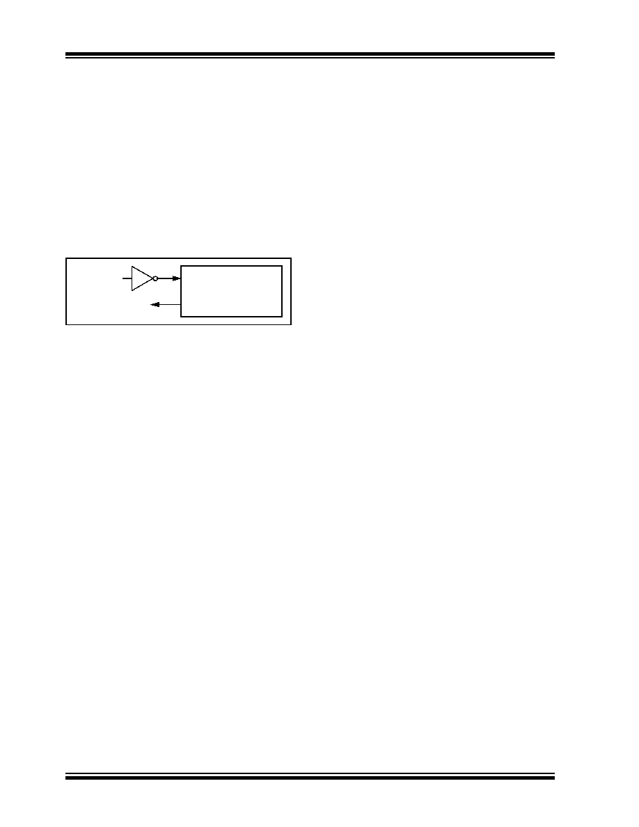
FIGURE 3-3:
EXTERNAL CLOCK INPUT
OPERATION (EC AND
ECPLL CONFIGURATION)
3.2.4
PLL FREQUENCY MULTIPLIER
PIC18F46J50 family devices include a PLL circuit. This
is provided specifically for USB applications with lower
speed oscillators and can also be used as a
microcontroller clock source.
The PLL can be enabled in HSPLL, ECPLL,
INTOSCPLL and INTOSCPLLO Oscillator modes by
setting the PLLEN bit (OSCTUNE<6>). It is designed
to produce a fixed 96 MHz reference clock from a
fixed 4 MHz input. The output can then be divided and
used for both the USB and the microcontroller core
clock. Because the PLL has a fixed frequency input
and output, there are eight prescaling options to
match the oscillator input frequency to the PLL. This
prescaler allows the PLL to be used with crystals, res-
onators and external clocks, which are integer multiple
frequencies of 4 MHz. For example, a 12 MHz crystal
could be used in a Prescaler Divide-by-Three mode to
drive the PLL.
There is also a CPU divider, which can be used to derive
the microcontroller clock from the PLL. This allows the
USB peripheral and microcontroller to use the same
oscillator input and still operate at different clock speeds.
The CPU divider can reduce the incoming frequency by
a factor of 1, 2, 3 or 6.
3.2.5
INTERNAL OSCILLATOR BLOCK
The PIC18F46J50 family devices include an internal
oscillator block which generates two different clock
signals; either can be used as the microcontroller’s
clock source. The internal oscillator may eliminate the
need for external oscillator circuits on the OSC1 and/or
OSC2 pins.
The main output (INTOSC) is an 8 MHz clock source
which can be used to directly drive the device clock. It
also drives the INTOSC postscaler which can provide a
range of clock frequencies from 31 kHz to 8 MHz.
Additionally, the INTOSC may be used in conjunction
with the PLL to generate clock frequencies up to
48 MHz.
The other clock source is the internal RC oscillator
(INTRC) which provides a nominal 31 kHz output.
INTRC is enabled if it is selected as the device clock
source. It is also enabled automatically when any of the
following are enabled:
Power-up Timer
Fail-Safe Clock Monitor
Watchdog Timer
Two-Speed Start-up
These features are discussed in larger detail in
The clock source frequency (INTOSC direct, INTRC
direct or INTOSC postscaler) is selected by configuring
the IRCF bits of the OSCCON register (Page 43).
OSC1/CLKI
OSC2/CLKO
FOSC/4
Clock from
Ext. System
PIC18F46J50
相关PDF资料 |
PDF描述 |
|---|---|
| PIC32MX775F512L-80I/BG | IC MCU 32BIT 512KB FLASH 121XBGA |
| PIC32MX795F512H-80I/MR | IC MCU 32BIT 512KB FLASH 64QFN |
| PIC18F6585-I/PT | IC PIC MCU FLASH 24KX16 64TQFP |
| C8051F206 | IC 8051 MCU 8K FLASH 48TQFP |
| PIC16C64A-20/L | IC MCU OTP 2KX14 PWM 44PLCC |
相关代理商/技术参数 |
参数描述 |
|---|---|
| PIC18LF4685T-I/ML | 功能描述:8位微控制器 -MCU 96KB FL 3KB RAM RoHS:否 制造商:Silicon Labs 核心:8051 处理器系列:C8051F39x 数据总线宽度:8 bit 最大时钟频率:50 MHz 程序存储器大小:16 KB 数据 RAM 大小:1 KB 片上 ADC:Yes 工作电源电压:1.8 V to 3.6 V 工作温度范围:- 40 C to + 105 C 封装 / 箱体:QFN-20 安装风格:SMD/SMT |
| PIC18LF46J11-I/ML | 功能描述:8位微控制器 -MCU 64KB Flash 4KBRAM 12MIPS nanoWatt RoHS:否 制造商:Silicon Labs 核心:8051 处理器系列:C8051F39x 数据总线宽度:8 bit 最大时钟频率:50 MHz 程序存储器大小:16 KB 数据 RAM 大小:1 KB 片上 ADC:Yes 工作电源电压:1.8 V to 3.6 V 工作温度范围:- 40 C to + 105 C 封装 / 箱体:QFN-20 安装风格:SMD/SMT |
| PIC18LF46J11-I/PT | 功能描述:8位微控制器 -MCU 64KB Flash 4KBRAM 12MIPS nanoWatt RoHS:否 制造商:Silicon Labs 核心:8051 处理器系列:C8051F39x 数据总线宽度:8 bit 最大时钟频率:50 MHz 程序存储器大小:16 KB 数据 RAM 大小:1 KB 片上 ADC:Yes 工作电源电压:1.8 V to 3.6 V 工作温度范围:- 40 C to + 105 C 封装 / 箱体:QFN-20 安装风格:SMD/SMT |
| PIC18LF46J11T-I/ML | 功能描述:8位微控制器 -MCU 64KB Flash 4KBRAM 12MIPS nanoWatt RoHS:否 制造商:Silicon Labs 核心:8051 处理器系列:C8051F39x 数据总线宽度:8 bit 最大时钟频率:50 MHz 程序存储器大小:16 KB 数据 RAM 大小:1 KB 片上 ADC:Yes 工作电源电压:1.8 V to 3.6 V 工作温度范围:- 40 C to + 105 C 封装 / 箱体:QFN-20 安装风格:SMD/SMT |
| PIC18LF46J11T-I/PT | 功能描述:8位微控制器 -MCU 64KB Flash 4KBRAM 12MIPS nanoWatt RoHS:否 制造商:Silicon Labs 核心:8051 处理器系列:C8051F39x 数据总线宽度:8 bit 最大时钟频率:50 MHz 程序存储器大小:16 KB 数据 RAM 大小:1 KB 片上 ADC:Yes 工作电源电压:1.8 V to 3.6 V 工作温度范围:- 40 C to + 105 C 封装 / 箱体:QFN-20 安装风格:SMD/SMT |
发布紧急采购,3分钟左右您将得到回复。